This article is part of the TechXchange: Exploring Op Amps.
Members can download this article in PDF format.
What you'll learn:
- Characterizing SSBW for VFAs and FDAs.
- What's hiding in some fully differential amplifiers?
- Measuring response shape and harmonic distortion.
- Adding an input common-mode control loop to a legacy FDA.
Industry amplifier development groups continue to improve on devices and analysis techniques, publishing those in datasheets, application notes, industry articles, etc. But these rarely find their way into textbook updates. Read on for a representative sample of what you might have missed in your EE education.
The classic gain bandwidth product (GBP) idea was always an oversimplification. One simple plot yields much closer SSBW versus gain prediction for any voltage feedback amplifier (VFA) or fully differential amplifier (FDA).
The well-known GBP model predicts that the closed-loop small-signal bandwidth (SSBW) will simply be the GBP divided by the noise gain (NG). The NG is the inverse of the voltage divider from the output pin back to the feedback input pin(s). In a non-inverting VFA design, the NG will be the same as the desired signal gain.
It doesn’t take very long in characterizing SSBW over gain for VFA amplifiers to find out that this model is not very close at lower gains. The model is assuming a single-pole loop gain (LG) condition, where that’s hardly ever the physical case. A second-order model gets much closer, but it too is still an approximation for most modern VFA op amps and/or FDAs.
Almost any modern (but accurate) VFA model can be used to illustrate these effects—even allegedly unity-gain stable devices. All IC designers (and most marketers) know that designing a unity-gain VFA op amp for about 65-deg. phase margin will give far higher closed-loop SSBW than the GBP might predict (≈1.55X). A nominal unity-gain, 65-deg. phase-margin design is very common, yielding an approximate closed-loop Butterworth design (at least second order by definition).
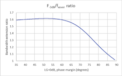
The approach to generate Figure 1 was to introduce a NG zero to a single pole Aol analysis by adding a tuning capacitor at the inverting node to ground for an inverting op-amp configuration. Solving for the loop gain (LG) = 0-dB point, as that zero is reduced in frequency (ramping that capacitor up), will yield one quadratic.
Then, at that same capacitor value, the LG phase margin is used to solve for the closed-loop second-order Q, and subsequently the resulting F-3dB. The ratio of that F-3dB to the LG = 0-dB frequency is formed to get Figure 1. Note that for phase margin < 65 deg., the closed-loop response will also be peaking.1
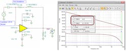
A good example can be shown using the OPA134 simulation model. Figure 2 shows the Aol gain and phase simulation,1 which would be the same thing as the LG plot for a unity-gain configuration.
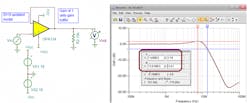
This simulation shows 54-deg. phase margin, which, from Figure 1, should give a close- loop gain of 1 SSBW extension to 7.79 MHz*1.61 = 12.54 MHz. The gain of 1 simulation in Figure 3 shows a 13.6-MHz F-3dB with 1.8 dB peaking. Ideally, a 54-deg. phase margin should be giving about 1.2 dB peaking (Fig. 2)1, so these results are close, but not exact, to the expected response shape due to higher-order poles in the model not captured by this second-order analysis.
The curve of Figure 1 adds a lot to our understanding of the closed-loop SSBW over gain versus the simple GBP model that would have predicted only 7.8-MHz F-3dB unity-gain bandwidth.
How do you really combine the distortion terms in cascaded amplifiers or amplifier + ADC systems? Legacy power summing calculations are quite incorrect.
One of the fundamental questions in an analog-to-digital converter (ADC) driver application is how low do the harmonic-distortion (HD) terms need to be coming into the ADC to only slightly impair its performance. Numerous early efforts at this simply added powers as if the individual distortion terms were in a 45-deg. (quadrature) relationship.
In fact, the individual input distortion terms must be added linearly to those same terms for the ADC itself. Extensive testing with individual FDAs (THS4509) and high-speed ADCs (ADS5500), where each device was separately characterized then combined, proved that the individual distortion terms add in phase as voltage vectors.2 The math combining two cascaded stages for each distortion term is shown as Eq. 1:
This is written as spurious-free dynamic range (SFDR), but actually the HD2 and HD3 (etc.) terms would be combined individually. Legacy literature would often report the combination as a total harmonic distortion (THD) power combination as in Eq. 2, which is totally incorrect (page 43, Ref. 3):
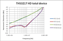
Much more recent bench testing of a two-stage amplifier (THS3217), where the input and output stages were measured separately, then combined in cascaded stages, showed these same results (Fig. 4). Here, the input D2S stage was tested over frequency with a 2 V p-p into 200-Ω load, while the OPS stage in that same unit was tested separately producing 5 V p-p into 100-Ω load.
These separate measurements were combined using Eq. 1 to predict the cascaded distortion. Then the same part was measured in a cascaded configuration producing the same swings and loading at each stage. Clearly, Eq. 1 appears to correctly combine the cascaded distortion performance.
Imagine coming into an ADC (or second amplifier stage) with a large fundamental carrier that has its own HD2, HD3, etc., harmonic distortion terms. The ADC (or second amplifier stage) will generate its own harmonic terms from the large fundamental and combine those “in phase” with the terms coming into its input. This makes the problem of minimal ADC degradation much more difficult than predicted by the legacy (and incorrect) power addition assumption of Eq. 2.
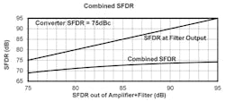
Sweeping Eq. 1 for a fixed ADC SFDR term and an improving input-signal SFDR term shows a slowly closing gap in Figure 5. For any ADC spurious term reported, degrading it by less than 1 dBc requires an input term at least 20 dB lower than the ADC reported number. This example was for a −75-dBc ADC spur, but it generally holds for any starting level.
The fully differential amplifier (FDA) combines a differential + common-mode (CM) control loop. Hiding inside some FDAs is a very low noise active balun capability.
The first FDA—the AD8138—emerged in 1999. It was an ideal solution for converting single-ended signal paths to the differential drive required by the high-speed pipeline ADCs that had started to emerge in the mid-90s. As FDA bandwidths increased (far beyond 4 GHz today), the need for a matched input impedance was obvious.
However, the FDA’s two-loop nature rendered the solution for the required resistors to provide that single-ended impedance match, as well as the desired differential gain, very elusive. In fact, both National Semiconductor and Analog Devices capitulated on that analysis4 and developed solutions that were in fact iterative to simultaneously match to some source impedance and deliver the desired gain.
Sinking deep into an algebraic morass in the 2012 timeframe, I extracted a closed form solution for the input resistor to ground (Rt) as Eq. 3:
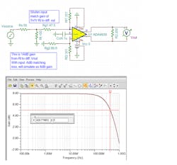
Figure 6 shows an example gain of 5-V/V design, first picking Rf = 301 Ω, then solving for Rt and subsequently the two Rg values to give a 50-Ω input match. The FDA CM loop will move the CM input voltages with the input signal to generate the output voltage on the non-signal input side. This has the effect of making the apparent impedance looking into Rg1 higher than the physical value (100-Ω active impedance in Figure 6).
With Rt solved, the series input gain resistor is then resolved for a selected Rf value.4 While Eq. 3 looks too complicated to be either correct or useful, it’s in fact both. In the original work, I tested these results against both the ADI and NSM tools, delivering identical results for the required R values. Starting with a selected feedback Rf value is required to apply current-feedback-based FDAs.
So, what does this equation offer over the equally effective iterative approaches? Recalling that this equation is for the (kind of extra) resistor to ground (Rt) at the input to attain an impedance match, what if we solved the denominator expression for a zero value? That will eliminate this extra Rt resistor to ground, leading to the lowest noise ac- or dc-coupled matched input impedance single-to-differential FDA interface.
Unlike typical magnetic baluns, commonly used in higher-frequency RF channels, this solution can be truly dc-coupled. This “active balun” solution offers a new signal-path processing option for single-to-differential requirements up to an ADC.5
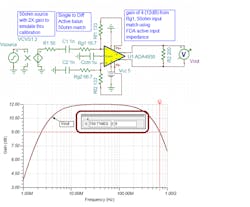
While the ISL55210 would be the lowest-noise (0.85nV/√Hz) device to apply here, Figure 7 shows an example design using the 1.4-nV/√Hz noise ADA4930. Here, the 2.4-MHz, lower F-3dB is set by the 1-nF blocking caps and could be lowered using higher capacitor values.
This 12-dB gain stage (from Rg1) gives about 200-MHz flat span with 700-MHz F-3dB. That Rg1 = 16.7 Ω is in fact providing a 50-Ω input match using the active impedance feature of a single-to-differential FDA stage.5 For this to work broadband, the internal CM loop bandwidth must be on the order of the differential loop—they are for these higher-speed FDAs. That CM loop bandwidth is much higher than the reported bandwidth from the control pin to the output CM voltages.
Running an output differential spot-noise simulation shows only 4.2nV/√Hz; the input refers to about 1 nV for this gain of the 4-V/V stage. The input referred noise here is actually less than the specified 1.4-nV FDA input voltage noise, since the signal gain of 4V/V is slightly more than the noise gain of 3 V/V. This 1-nV input spot noise translates into 7.8-dB noise figure for a 50-Ω source and Ta = 17°C.
How would you really interface from an FDA to an ADC while also implementing a direct response shape or harmonic-distortion measurement with the ADC input pins down to −110-dBc levels?
The significant effort devoted to delivering a very-low-distortion input signal to an ADC, with some desired frequency-response shape, then combines with the ADC distortion and frequency response terms. Differential probes can be used at the ADC inputs to verify the response shape or step response, but they don’t have the dynamic range to extract out the distortion performance for the best interfaces.
Starting from a simple RLC interstage filter7 design (adapted to differential for an FDA-to-ADC design), that last parallel resistor across the ADC inputs can be split into a very high-dynamic-range differential to single-ended test port to measure the response shape and harmonic distortion right at the ADC inputs.
These ideas show up in a fully developed and tested evaluation (EVM) boards using a 4-GHz low-noise FDA (ISL55210) with a 14-bit, 500-MSPS ADC.8 The aim was to provide a flat 100-kHz to 100-MHz gain of 15-dB interface with minimal signal-to-noise ratio (SNR) and SFDR degradation over the ADC-only specs. That was achieved indicating the SFDR at the ADC inputs was ≤110 dBc through 100 MHz driving 1.8 V p-p differentially at those ADC input pins.
The RLC filter design was necessarily a bit iterative as both the board parasitics and ADC input C were somewhat uncertain. The RLC filter design intentionally targeted a final differential C at about 2X the ADC reported internal value to enable some range for tuning the final external C value down.
That proved trivial as the exact response shape to the ADC inputs (while sampling) was available through the interface described here. Board-level tuning on that last C reduced it to only 1 pF. This signal sense technique can be applied right at the input of any ADC interstage filter design with good results. It’s necessarily ac-coupled but suitable for the intended network- or spectrum-analyzer measurements.
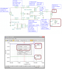
While the starting point for this RLC filter design is second order,7 the design went third order with that added differential C right after those first resistors (Fig. 8).
Going left to right in Figure 8:
- The FDA differential outputs drive the filter with an output common-mode dc voltage that optimizes the SFDR out of the chosen FDA (1.65 V here, for example)
- Those first small 40.2-Ω resistors isolate the FDA outputs from the reactive loading of the LC elements. They will also introduce a small insertion loss in the filter to the final differential Rload (−2.45 dB here).
- To isolate common-mode voltage setups from the FDA to the ADC, series 1-μF blocking caps are inserted in the signal path. This is okay for the measurements here, but the interface could also be dc-coupled to the ADC input pins with a bit more effort.
- The differential C, series L’s and total final differential C form the third-order filter. This ADC specified a 300 Ω||9 pF differential input Z where an external tuning Ctune is added to fine-tune the filter flatness in this simulation (it also is used to fine-tune the measured response flatness in the final EVM8).
- The filter design called for a final single-ended R of 122 Ω. With half of the ADC’s internal 300 Ω forming part of that, the external single-sided R’s needed to be 662 Ω. The sense path interface passes through a differential-to-single-ended balun conversion (here using the Mini-Circuits ADT1-1WT) to a final 50-Ω measurement instrument termination. That reflects back to the input side of the balun as 25 Ω on each side in parallel with the physical 26.7 Ω. Those combine to 12.9 Ω to form a total of 12.9 Ω + 649 Ω = 662 Ω as required for the filter design.
- The actual design flow for those two resistors targets a total input resistance, including the reflected 25 Ω from the test instrument, and sets a source impedance (26.7 Ω||649 Ω) looking back from the balun primary matching that’s 25 Ω for each side on the balun inputs (50 Ω total).
- Since blocking caps are in the signal path, the required ADC input Vcm can be brought in at the junction of the two 26.7-Ω resistors (0.95 Vcm here).
The frequency response to the ADC inputs shows about ±0.3-dB flatness through 100 MHz (tuning this with the external Ctune), while the sense path at the balun output is a very near replica in shape with considerable attenuation. That measurement path loss is fine for response or harmonic distortion measurements. For lower-frequency spans, use the ADT1-6T.
This approach can be adapted to other design requirements, with the only requirement being a relatively large differential resistor at the ADC inputs broken into this differential-to-single-ended sense path structure. Reference 8 shows measured results using this circuit, revealing that fast Fourier transform (FFT) distortion performance is slightly better than the ADC-only specifications.
Once we have the single-ended version of the ADC input voltage available at the balun output, several harmonic-distortion measurement methods may be applied. Simple spectrum-analyzer measurement will get down to about −90-dBc levels, whereas source cancellation approaches will drop down to better than −110 dBc.9
Legacy FDAs struggle with background CM signals on both inputs. A newer solution adds an input CM control loop along with the classic FDA design.
One of the more interesting problems that crops up occasionally is to implement a differential transimpedance stage instead of an FDA when the latter would seem to be applicable. Often, what’s made this more problematic is if the two source currents have a large and varying CM current on top of the differential signal.
If that CM current is constant, sometimes we bleed that off at the input summing junctions with fixed resistors to some supply. That, of course, increases the dc noise gain and injects whatever noise is on the reference supply. And it won’t work if that CM current varies with time.
The obvious, but previously unavailable, solution is to add an input servo loop that sums equal CM currents into the input nodes to hold an externally set “input” CM voltage. The new (released Dec. 2020) THS4567 starts out with a relatively fast 220-MHz, GBP decompensated core FDA structure and then adds this input servo loop to absorb the source CM current terms.
Since it’s intended for differential transimpedance applications from detector diodes, the decompensated FDA is more suited to that application, where the first job in any design is to get the feedback Cf set for the desired frequency response, usually Butterworth. A simple solution for compensating a transimpedance design for the required feedback Cf to achieve a closed-loop Butterworth is as follows:10
First, get the approximate noise gain zero dropping out the feedback Cf from this equation for Z1, where Cs is the total capacitance on each input pin:
The characteristic frequency for the second-order closed-loop response will be given by:
Where we need to be using the true single-pole GBP in this equation.10
Then, to set the feedback pole location (P1), use this relationship, where Fc is the intersection of the higher frequency noise gain (1+Cs/Cf) with the GBP curve, but use the P1/Fo part of this here:
Setting P1 (the feedback pole) to get a Q = 0.707 (Butterworth) will then yield an F-3dB = Fo.
Stepping through this with a desired 1 MΩ on each side gain for the THS4567 with 10-pF detector diode capacitance will give:
- Z1 = 1/(2π*1 MΩ*11 pF) = 14.47 kHz (where I’ve added 1 pF for the THS4567 input C on each side)
- Fo = √(14.47 kHz*220 MHz) = 1.78 MHz = F-3dB (if Q set to 0.707)
- P1 = 0.707*1.78 MHz = 1.2 6MHz, Cf = 0.12 pF
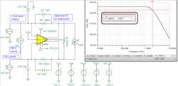
The response certainly looks Butterworth, with almost exactly the expected 1.8-MHz F-3dB for this 2 MΩ (126 dBΩ) design (Fig. 9).
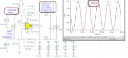
Resetting the feedback Cf to a typical thick-film resistor 0.18-pF parasitic, and adding a 10-MHz post RC filter, shows the ±4-V differential output of Figure 10 for a ±2-μA, 100-kHz sine-wave input sitting on top of 50-μA CM input current. Without the input cancelling currents, that 50-μA CM current would be taking the outputs to negative 50 V.
Here, I had set the target input CM voltage to 1.0 V with the output Vocm midsupply at 2.5 V. Each output is swinging ±2 V around that to give the ±4-V differential output for the ±2 μA shown in Figure 10.
This device might also be used to gain up a small differential voltage signal on top of a larger CM source voltage that varies with time. In this case, the maximum input Icm current for the CM voltage range must be less than the maximum available internal Icm cancelling current. The specification doesn’t appear in the datasheet, but up to 1 mA is supported in the simulation model.
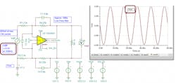
Backing that maximum off to a safe ±800 μA maximum, use that to design a gain of 10 stage with ±2-V input CM range. That will then require a 2-V/0.8-mA = 2.5-kΩ input resistor with a 25-kΩ feedback Rf.
These higher R’s will require some compensation. Here, I’ve added a feedback Cf to give a 1-MHz pole, then added a differential input C that will shape the noise gain to 10 V/V at higher frequency (Fig. 11).12 The input Icm servo loop cancels the input 800 µA of CM current to hold the input pins at 1 V. Those two Icm currents do have some offset introducing an output offset voltage in this simulation.
This brief survey of some of the newer results coming out of the various amplifier development groups just touch on the vast range of newer (and hopefully better) analysis approaches and devices that have emerged over the last 10 years. Many more exist, but they require a close reading of the vendor material to expand your horizons. Someday, most of these might appear in an updated textbook.
Read more articles in the TechXchange: Exploring Op Amps.
References
1. Stability Analysis for High Speed Amplifiers – The Signal Sped Up, Insight #5
2. TI Training Seminar – Selecting the Right High-Speed Amplifier to Drive High Speed ADC’s
3. Legacy literature showing a combined THD as a power addition
4. Analog Devices Diff Amp Calculator
5. Wideband matched input single to differential active balun using an FDA
6. Active balun EVM using the ISL55210 videos
7. Low insertion loss RLC filter for ADC driving
8. 14bit, 500MSPS ADC with FDA and filter EVM
9. Source cancellation harmonic distortion measurement
10. Transimpedance Design for High Speed Amplifier Application Note
11. Why is Gain Bandwidth Product so Confusing?
12. Unique compensation technique tames high bandwidth voltage feedback op amps
