Members can download this article in PDF format.
What you'll learn:
- The top strategies to overcome miniaturization issues in PCB assembly.
- Examples of successful miniaturized PCB applications.
- Frequently asked questions about PCB miniaturization.
In Part 1, “Top 5 Challenges in PCB Assembly,” we examined the five main challenges facing PCB designers. These include signal integrity and thermal management, bare-board production, PCB assembly and placement, advanced materials and smaller components, plus rework and repair.
While these challenges are daunting, they can be mitigated with systematic planning, optimized designs, advanced processes, quality control, and expertise in PCB design, manufacturing, and assembly. What follows are five strategies often used to deal with miniaturization issues in PCB assembly (see "Frequently Asked Questions" below for more on the benefits and challenges of miniaturized PCBs).
1. Optimized PCB Layouts and Proper DFM
Adding thermal vias for heat dissipation, isolating high-speed signals, enabling access to test points, and incorporating design-for-manufacturing (DFM) principles are all examples of careful layout strategies. Such enhancements reduce the difficulties in PCB production and assembly and improve manufacturability. Generally speaking, a good design is critical for successful PCB production, especially for such high-density and high-tech circuit boards.
2. Skilled Workforce and Engineering Expertise
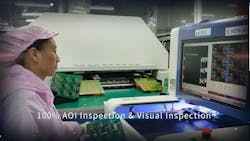
Very skilled workers are needed to handle miniaturized printed circuit boards, such as in drill, etching, lamination, and plating processes in PCB production; solder-paste printing; SMT pick-and-place; and reflow soldering processes in PCB assembly (see figure).
Besides, extremely experienced engineers are needed to check the customers’ designs and prepare production files. These engineers know the production very well and can foresee and avoid possible mistakes in advance. Likewise, the engineers should collaborate closely with designers early on to optimize manufacturability. Such expertise is essential for quality and efficiency.
3. Advanced PCB Production and Assembly Equipment
For ordinary circuit boards, general circuit-board production and assembly equipment are sufficient. But for miniaturized and high-density circuit boards, use of advanced high-precision equipment is necessary.
In PCB production, we need to use laser drill machines, advanced pattern imaging, and etching, plating, and lamination equipment. Furthermore, the inspection and testing apparatuses need to be more advanced to be suitable for PCBs with small drills and traces.
In PCB assembly, highly precise and high-speed pick-and-place equipment is used to place the components on the PCBs correctly and quickly. Then, high-accuracy nozzles, optical alignment systems, servo-mechanisms, and miniaturized components can be reliably placed. Pulsed-gas nozzles, for example, reduce placement impact, while pattern recognition accurately aligns parts.
4. Complete Quality Management in Production
Even with very experienced employees and very advanced equipment, it doesn’t mean that qualified circuit boards can suddenly be produced. Quality control in the production process is critical. From incoming material to finishing of final products, we need to confirm that the PCB production and assembly process is carried out in accordance with international quality-management standards, such as ISO9001, ISO13485, UL, etc.
5. Adequate Testing and Inspection
After the circuit boards are finished, we must also do lots of testing to confirm that the product meets the international acceptance standards, such as IPC-A-600 for printed circuit boards and IPC-A-610 for PCB assembly. On top of that, we should always pay attention to a customer's own acceptance standards.
Common tests currently include IQC (In-coming Material Inspection), AOI (Automated Optical Inspection), microsection inspection, electrical open and short test (E-test), impedance value test, solderability test, ICT (In-circuit Test), FCT (Functional Test), X-ray check, and visual defects inspection, among others according to customers' requirements.
Inspiring Examples of Miniaturized PCB Application
Despite the challenges, some inspiring product examples highlight the tremendous capabilities enabled by miniaturized PCBs. For instance, CochlearTM hearing implants use flexible miniaturized PCBs to interface electrodes with the auditory system comfortably and non-invasively. The intricately folded PCB assembly fits perfectly inside the ear canal for natural hearing sensations.
Likewise, electronic smart contact lenses from Mojo Vision incorporate extremely thin, transparent, and flexible printed circuit boards. These nearly invisible PCBs enable discreet head-up displays on the lenses for connected augmented-reality applications.
Dexcom's continuous glucose monitoring sensors employ miniaturized PCBs to mount the sensor electronics on a thin peel-and-stick patch comfortably worn on the skin. The accurate real-time glucose measurements are transmitted wirelessly to a receiver device.
Medtronic's advanced pacemakers feature integrated miniaturized PCBs encapsulated using proprietary epoxy and plastics. This ensures biocompatibility while protecting the delicate electronics operating within the human body.
Such examples highlight the broad scope of innovations possible thanks to progress in miniaturized PCB implementation. As technology advances, we can expect more such products that enhance functionality and user experiences through clever miniaturization.
The Future of Miniaturized PCBs
The rising prominence of miniaturized PCBs faces multiple challenges like small traces and vias on PCB bare board, precision component placement, thermal management, signal integrity, solder-joint reliability, and rework difficulties. However, through deliberate design strategies, advanced equipment, complete quality-control processes, adequate testing and inspections, skill-building, and engineering collaborations, these hurdles can be overcome to realize the benefits.
As miniaturization and high-density PCB fabrication and assembly technologies mature further, we can anticipate their widespread adoption across industries. The future points toward a “small” yet powerful era of electronic innovation, where tiny PCBs deliver amazing capabilities and enable novel applications limited only by human imagination.
Read more articles in the TechXchange: PCB Tools and Technology.


