Members can download this article in PDF format.
What you’ll learn:
- Inefficiencies for OEMs to use PDF-only datasheet documentation of integrated circuits.
- Standards that address electronic documentation for I2C, SPMI, SPI, and JTAG devices.
- ROI: Faster volume sales and internal IC ATE reuse of electronic documentation.
This article is intended to help educate the component supplier community, help prepare suppliers for Veoneer’s requirements, and educate readers on the new requirements needed to do business with OEMs developing complex electronic systems.
It describes why and how Veoneer went from solely using PDF engineering documents to specifying and receiving standards-based computer-readable documentation for on-chip registers found in the components that we purchase. The method is similar to how the industry moved from PDF documents for dimensionalized drawings of component bodies to supplying electronic files for component bodies in 3D formats such Initial Graphics Exchange Specification (IGES) or Standard for the Exchange of Product (STEP).
The best method is to let the OEM customer use the electronic engineering data directly, rather than manually reading, re-interpreting and re-entering supplier engineering data. Our customers produce the safest vehicles in the world; therefore having a formalized approach to electronic component specifications benefits everyone involved from suppliers, to OEM engineers to ultimately, vehicle drivers and pedestrians.
Overview
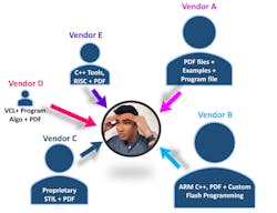
Here at Veoneer, we purchase CPUs, SoCs, FPGAs and an entire ecosystem of components needed to support these devices in our automotive based products. In the past, each component supplier provided their own ad-hoc documentation formats (Fig. 1).
We would get PDF files, sometimes an evaluation board, other times a proprietary software application with GUI, still other times value change dump (VCD) or XML files, and occasionally C/C++ examples are provided (Fig. 1). The engineering cost of digesting all of that information increases logarithmically with the complexity of the components, the number of components, and the technology utilized by the components.
Just one component that’s used in our system may have a 1,000-page PDF (Adobe Portable Document Format) file of documentation provided by the component supplier. Our engineers then need to read and understand it to become familiar with each technology interface (LDOs, ADC, SERDES, MIPI, NAND, DDR5, etc.) being used in the component. Past experience has shown that getting the supplier documentation in this ad-hoc fashion, from a dozen different suppliers, isn’t scalable.
The learning curve for new devices is steep. It becomes an impediment to fast system bring-up, thorough system evaluation, and speedy ramp-up to volume production. In extreme cases, the complexity and difficulty may even cause a given project to get cancelled.
Customer projects that never get to production are losses for the component supplier. The supplier has upfront sales and support time costs and other NRE that will never be recouped from device sales when the customer’s product doesn’t reach volume production.
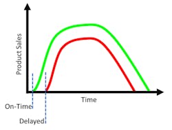
Component suppliers, therefore, also can benefit from a solution that speeds up the OEM’s engineering tasks. OEMs that can quickly take new components and launch new systems into high-volume production can generate revenue earlier (and greater) for themselves, but also for the component supplier. In Figure 2, the on-time start (green line) shows greater product revenue. The delayed (red line) graph shows less revenue is possible. The graph applies to both the OEM and component supplier.
Hence, it’s in the component supplier’s best interest to ensure that the domain expertise in the silicon’s functionality is transferred to the OEM correctly and in a standardized manner that’s computer-readable and verifiable.
The Goal
It shouldn’t take more than 15 minutes of engineering time to interact with a new IC. Within 15 minutes from power-up, an engineer should be able to set the voltage level of any pin, read the voltage present at the input of any ADC, and alter the contents of any on-chip non-volatile memory (NVRAM or flash). In other words, the engineer should be able to connect to an industry standard serial interface, power-up the device and read/write any register, pin, or on-chip memory.
However, the reality is that it can take tens of hours to achieve it. And it can take possibly hundreds of hours (with lots of meetings) when things go wrong. The OEM is typically forced to absorb the schedule delays and costs even if the thing that went wrong was the result of poor documentation.
OEMs can’t achieve that 15-minute goal with PDF documentation given the complexity of today’s ICs. That complexity is further exacerbated by the great variety of methods used to program on-chip non-volatile memory.
Standards-Based Computer-Readable Documentation to the Rescue
Simply stated, the approach we use today removes the sole reliance on PDF or Microsoft Word technical documents to describe the associated registers in a system-on-chip (SoC) or IC. We specify IEEE 1149.1-2013 and IEEE 1149.10-2017 based documentation to our suppliers for all components that have a serial interface such as I2C, SPI, SPMI, RFFE, or SerDes.
The first mentioned standard, 1149.1-2013, defines how to describe on-chip registers (via the new highly revised hierarchical BSDL language) and how to operate them (via a language called procedural description language or PDL).1 The second standard mentioned, 1149.10-2017, shows how to define industry or MIPI standard serial interfaces that can read and write these on-chip registers.
When documentation is delivered in these IEEE approved formats, then the OEM can use commercially available tools to read the vendor-supplied files and operate the IC. This capability is then enabled across all engineering segments in our company, design bring-up and validation, production test, and field return. These resources are spread out across multiple geographical locations.
Did You Say, “We don’t have JTAG in our chip!”?
Don’t let the description on the use of boundary scan description language (BSDL) trip you up. BSDL started out in life as a description for 1149.1 or “JTAG” device boundary registers way back in 1993. It was substantially overhauled (I mean really substantially) in the 2013 standard.1 BSDL now supports a description hierarchy of IP blocks and high-level descriptions of all test registers inside of a modern IC. In addition, it supports describing any imaginable IEEE 1500 fabric inside of an IC.
So, think of it as having more focus on the “SDL” or scan description language today rather than the “boundary” portion back in 2001. If your engineers only know the old JTAG from 2001, then it’s like comparing know-how on the combustion engines of 2001 to the know-how needed for electric vehicles of today.
BSDL also is used by IEEE 1149.10-2017.2 This standard leverages the hierarchical chip-register descriptions in BSDL and dispenses with the requirement to have anything else in the IC design related to the IEEE 1149.1 standard. This was done to solve two problems.
The first problem to overcome was enabling a serial channel such as I2C, SPI, SPMI, or RFFE as the data-transport mechanism instead of JTAG. That’s accomplished by the 1149.10 standardization of mission-mode serial interfaces via add-on attributes to BSDL. The second problem was the hefty requirement for designers to connect up DFT-based registers needed by 1149.1. That problem solved itself by enabling descriptions of on-chip registers via (B)SDL and enabling the description of common serial interfaces.
There’s no need for special DFT or test specific registers with 1149.10-2017 when common synchronous serial interfaces are used. The normal mission-mode registers IC supplier documents in PDF can now be documented via these IEEE standards!
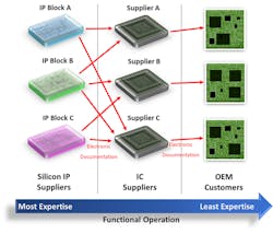
Figure 3 shows the basic overview of how this approach is used in the industry. When I presented this approach, my managers said, “It makes perfect sense. Why aren’t we doing this already?”3 To be fair, I didn’t invent all of this, but I have had some great teachers.4
After working at several major OEMs in my career, I can see where common sense should be applied to lower the cost of engineering. The makers of the IP blocks, the logic cores, and I/O technology know best how their design works. They have the most “Domain Expertise,” so that’s where the electronic documentation should start (see blue arrow at the bottom in Figure 3).
An electronic manufacturing service (EMS) used by an OEM customer has domain expertise elsewhere. They know the least about how the functionality works due to the hundreds of technologies they’re exposed to every day. It’s like brain-surgeon doctor versus general-practitioner doctor. The GP is going to have good knowledge across all of the body parts and the brain surgeon is going to be highly specialized in issues of the human cortex.
The other way to look at this is the IP providers and IC suppliers have the most number of end-users to amortize the cost of developing the electronic documentation. The OEM customer may only use the IC one time on one project. The cost of development can’t be distributed, and that development time comes at a critical juncture in the schedule when a new system is brought up. We may not know what’s wrong early on—either an incorrect interpretation of how a register works, or an issue in the target we have built, or it could be a subtle firmware issue.
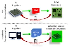
The other advantage with electronic documentation is the OEM customer is removed from the validation loop. On the top half of Figure 4, the classical flow is shown where the IC supplier provides PDF. The OEM’s engineer then reads it and interprets the PDF. If there’s an error or ambiguity, it’s fed back to the IC supplier. It usually is clarified through a series of supplier-customer meetings and updated documentation. The elapsed time to resolution can be quite large, causing that delayed entry shown back in Figure 2.
The better way is shown on the bottom half of Figure 4. The OEM customer is removed from the validation loop. The IC supplier can create the documentation and validate it against the IC or a simulation of the IC using commercial software. Once that validation is complete, the BSDL and PDL information can then be shared with the OEM customer. The validated electronic documentation also can be shared with the IC supplier’s internal IC ATE team or Outsourced Semiconductor Assembly and Test (OSAT) to use as the basis for IC test-pattern generation and silicon bring-up on ATE.
A similar approach can be taken in the silicon IP supplier and IC supplier relationship. In that scenario, the silicon IP supplier validates the files they create against the IP block (ADC, NVM, etc.) prior to supplying the electronic documentation to their customer, the IC supplier.
How It Helps Us
The electronic documentation creates a baseline for us to always be able to operate the device. This baseline operation can be used during system bring-up before firmware is available or stable. It can be used by firmware engineers to make comparisons when things don’t work as expected. Or it can be employed at times where firmware isn’t present, as it may be during manufacturing test.
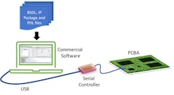
Since the documentation is in a standard format available to any software vendor, we have our pick of commercial software vendors to get the functionality we need. The software compiles the electronic documentation, and via a commercial USB serial controller, it converts the data to SPMI (or SPI, I2C as needed) protocol to communicate to the IC (Fig. 5).
The engineering task to get the IC to do something (i.e., return an ADC value, or program a NVM) becomes straightforward. We can write and read the on-chip registers, I/O, and NVM without becoming experts in the supplier’s target CPU, IC architecture, or IC specific technology.
PoC Phase Complete
We developed a proof-of-concept (PoC) using an older-generation power-management IC (PMIC), Qualcomm’s PM8916. We chose this as the functional register documentation was publicly available.5 The PM8916 also appears on the DragonBoard 410C—the PCB and all documentation also are publically available.6
The PoC was useful in validating that the languages in the standard were robust enough to support:
- Describing memory-mapped registers
- Allowing for instance-based hierarchy
- Use on existing or legacy devices without design changes
- Descriptions of SPMI and other serial protocols we use
Due to the nature of SPMI and SPI, where the length of the data shift changes depending on the type of data read/write operation (one byte, two bytes etc.), it was critical that the IEEE standard BSDL language and the software tools we selected could support this. We chose software from Intellitech to compile the IEEE 1149.x documentation and communicate to the target. Their tools support IEEE 1149.1-2013 and IEEE 1149.1-2017 file formats (BSDL with hierarchy and PDL) and can communicate to various serial interfaces such as SPMI, which is used in Veoneer systems.
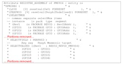
On each objective, the PoC was successful. The memory-mapped registers were described in “BSDL package” files, so they were self-contained for each peripheral, then instantiated into the top-level BSDL for the PM8916 (Fig. 6).
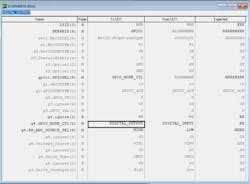
The 1149.10-2017 construct allowed us to use a commercial USB controller for communicating via SPMI. Using the BSDL and software as shown in Figure 5, we have an easy way to peek or poke any register interactively (Fig. 7). However, that capability doesn’t get us entirely where we want to go. The PDL language of IEEE 1149.1-2013 is used to describe more complex sequences.
As shown in Figure 8, several register values must be set to get a GPIO to change state. Drive-strength, drive-type (CMOS or LVTLL), and enable registers all have to be programmed to get the result. It makes for quick engineering work when the IC supplier works this out already and communicates the sequence to us in IEEE 1149.1-2013 PDL format. It’s just six registers that must be touched for a GPIO. As you would imagine, though, it gets far more complex for analog-to-digital converters (ADCs), temperature monitors, and advanced configurable I/O.
IEEE 1149.1-2013 PDL is a robust way to communicate the operation of even more complex on-chip targets. The IC supplier may specify something like the following equation for converting an on-chip voltage to temperature in degrees Celsius:
V = (kT/q) × ln(10) × 10
More work is required of the OEM customer when an equation like this is described only in PDF. The OEM engineer has to go about implementing that equation in software, just to know the on-chip temperature during board bring up.
When PDL is provided (Fig. 9), the OEM customer can execute the PDL and get the intended result without a lot of engineering work. There’s no need to read the PDF and then use engineering time to convert the formula (and debug and validate it) to something usable. The PDL will document the sequences that a software tool needs to take so it becomes immediately usable.
Similarly, Veoneer doesn’t want to become experts on how to program the NVM of a supplier’s IC. Our goal is to put values into the IC for trim or customization, not to be NVM programming experts. When NVM programming sequences are delivered as IEEE 1149.1-2013 PDL (or IEEE 1149.10-2017 PDL if it’s an i2c/SPI interface), we meet the objective of being able to program custom values into the IC within just a few minutes.
Advantages
The standards documentation approach has the following advantages:
1. Less engineering for both OEM and IC supplier
- Supplier gets PDL and IEEE 1149.x package files from IP supplier
- Supplier reuses documentation for IC ATE bring-up
2. Reduced documentation errors for customer
3. Impartial comparison result during OEM system bring-up
4. Firmware correlation during OEM bring-up and functional test
We’ve covered the first two items extensively. The third item refers to having the ability to always get a response or result from the IC, independent of what stage or state our system is in. The fourth item is somewhat related in that the firmware development team also has this additional data point to exploit. They haven’t had this data in the past, whereby they can review and compare a result that doesn’t on the CPU.
Conclusion
With the success of our internal PoC demonstration, I wrote an internal requirement for ICs that use the IEEE 1149.1 TAP and a second requirement document for devices with industry-standard serial interfaces. These documents specify the standards IEEE 1149.1-2013, IEEE 1149.6-2015, and IEEE 1149.10-2017, with some added Veoneer specific requirements where the IEEE standard has made a feature optional or hasn’t provided explicit guidance.
The set of requirements has become mandatory into component requirement specification (CRS) and application lifecycle management (ALM) for all product segments such as vision, radar, ADAS ECU, and others. We’ve had much dialogue with semiconductor suppliers to align on the value proposition and how it plays into Veoneer’s internal “Digital Test Strategy for Product Design Validation and Test Deployment.”
We’ve received feedback from our semiconductor suppliers as they begin to see the value proposition, scalability, and reuse that benefits their internal IC test as well. Insightful semiconductor sales managers are keen to see that faster production ramp-up for the OEM using these methods means volume IC orders sooner rather than later. Formal IC specifications in a standardized electronics format add real value to the industry. And since we’re in the vehicle safety business, ultimately that value can be measured in human lives saved.
References
1. https://www.intellitech.com/jtag/IEEE-1149-1-2013-Tutorial-Test-Re-use-from-IP-to-Systems.pdf
2. https://www.intellitech.com/bsdl/ieee-1149-10-tutorial.pdf
3. Special thanks to my mentors, Christer Rihs for being a technical and tactical adviser, and Mikael Johansson for being a sponsor and strategic adviser.
4. Credit here should be given to CJ Clark of Intellitech Corp. As chairperson of IEEE 1149.1-2013, he devised probably 95% of the architecture and grammar for BSDL and PDL to support this reuse approach; what he calls WORM, Write-Once-Read-Many. “Domain Expertise” and some of the figures and concepts in this article are derived from presentations he has given and are used with permission. My understanding from discussions with working group members was that he was the driving force behind all of it. I saw the same thing first-hand as a working group member in IEEE 1149.10-2017. CJ Clark was chair and editor and single-handedly architected the entire standard, wrote it, and showed us each week what he wrote. He devised a way to have the TAP and boundary scan register optional and invented a way to use SerDes as a test interface.
5. https://developer.qualcomm.com/qfile/29368/lm80-p0436-36_a_pm8916_hrd.pdf
6. https://www.96boards.org/documentation/consumer/dragonboard/dragonboard410c/hardware-docs/
