The U.S. Commerce Department signed a partnership with Alphabet’s Google to produce chips that startups, researchers, and universities can use to affordably design new types of semiconductors.
The deal brings the technology giant together with the National Institute of Standards and Technology (NIST). The agency said that researchers at its university partners will contribute the chip designs.
As part of the partnership, Google agreed to cover the expenses of setting up production as well as for the first run of chips, in a bid to speed up and bring down the cost of prototyping and then product integration.
The chips will be fabricated in the Bloomington, Minnesota, facilities of U.S.-based SkyWater Technology.
By making it more affordable to prototype and test chips before bringing a new product to market, NIST said it hopes to dramatically reduce the cost of semiconductor research in the U.S.
The deal comes as the U.S. prepares to dole out tens of billions of dollars in subsidies, grants, and other incentives under the recently passed CHIPS and Science Act. The Commerce Department recently said it plans to reserve $11 billion of the $52 billion in funding from the CHIPS+ Act for research and development (R&D), with a goal of “reestablishing this sector as the engine of innovation for the U.S. domestic economy.”
Chips At a Discount
Modern semiconductor design is an expensive undertaking. The cost to manufacture a prototype of a chip design before it enters mass production can climb to hundreds of thousands or millions of dollars.
Most major semiconductor firms engage in early-stage research to help remain competitive long term, and many have billions of dollars of resources that give them relatively ready access to prototype and test chips.
But the costs can be prohibitive for startups, universities, and researchers looking to try out innovative approaches to semiconductor design. As a result, it makes the endeavor too risky or impractical for them to invest time into.
The new program aims to reduce the cost of these chips dramatically by making open-source blueprints available for others to build on top of, while Google pays to get the physical parts manufactured in fabs, NIST said.
Said Under Secretary of Commerce for Standards and Technology Laurie Locascio, “By creating a new and affordable domestic supply of chips for research and development, this collaboration aims to unleash the innovative potential of researchers and startups across the nation.”
Google has been a prominent presence in open-source software for years. But it has also been investing in open-source hardware in recent years. The company’s pact with the U.S. government resembles its existing Open MPW program: It supplies open-source software tools for startups and universities to design, verify, and test virtual versions of the chips and then takes over the cost of manufacturing the physical silicon for them.
Last month, Google said it partnered with GlobalFoundries and the U.S. Department of Defense to expand the effort. SkyWater also provides capacity in its fabs to manufacture chips under the Open MPW program.
New Lab Partners
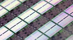
SkyWater will produce the chips on 200-mm wafers, which universities and other purchasers will have to dice into separate dies, assemble into packages, and test the final chips at their own processing facilities.
Giving researchers access to chips in the industry-standard format will allow them to prototype chips that can be quickly shifted into production, speeding up technology transfers from lab to market, NIST said.
As part of the partnership, the chips will be open source, which means that underlying blueprints will be open for others to copy, replicate, and adapt for their own purposes or specific applications and markets.
While it's unclear what process technologies will be used, the chips will likely be produced on the legacy nodes that are Skywater's specialty. The U.S.-based contract chip maker offers 90- and 130-nm process nodes, and it has also qualified a 65-nm node.
The Commerce Department said that as part of the new program, it "anticipates designing as many as 40 different chips optimized for different applications. Because the chip designs will be open source, researchers will be able to pursue new ideas without restriction and share data and device designs freely.”
Research partners contributing to the chip designs include the University of Michigan, the University of Maryland, George Washington University, Brown University, and Carnegie Mellon University, NIST said.
Though the collaboration with Google came about before the CHIPS Act passed, she said that it's an “example of how government, industry, and academic researchers can work together to enhance U.S. leadership in this critically important industry."
The terms of the agreement were not announced.

