Download this article in .PDF format
This file type includes high resolution graphics and schematics.
All high-speed analog-to-digital converter (ADC) datasheets show specified performance that really should be considered an ideal response under the best of all possible test conditions. Most systems can’t use coherent sampling, super-narrow bandpass filtering, or very high insertion-loss filters just before the ADC.
Upon realizing that those ADC datasheet numbers can’t be achieved in real systems, designers then must take an asymptotic approach. This can involve analytic tools, but will still probably require some iteration on the final interstage filter design to trade off the confluence of numerous issues.
High-speed ADC suppliers move mountains to extract the best signal-to-noise ratio (SNR) and spurious-free dynamic range (SFDR) performance in lab and automatic test equipment (ATE) tests for their converters. A very real “arms race” exists among chip suppliers to achieve the best numbers for their respective datasheets.
Nevertheless, it’s highly unlikely that any real system will reach those numbers. Therefore, the best designers can hope for is to not throw away any more dynamic range than is absolutely necessary. To do that, one must have intimate knowledge of the unusually constrained ADC characterization environment, along with the techniques for holding onto as much of that intrinsic capability as possible in an actual product.
In The Lab
High-speed ADC manufacturers have all evolved similar methodologies for device characterization, most of which are in the form of single-tone or multi-tone fast Fourier transform (FFT). The key results collapse down to a few numbers: SNR, SFDR, harmonic distortion (HD), and equivalent number of bits (ENOB).
At the most basic level, pulling the best SNR out of an ADC typically requires:
- Extremely low phase-noise source and clock
- High clock-signal amplitude to get through the sampling threshold as fast as possible
- “Coherent” sampling, which involves phase-locking the clock to the source and digitizing an integer number of input cycles; this removes the need for “windowing” in the FFT, reducing spectral leakage
- Driving the ADC from very low source impedance, which helps minimize Johnson noise from the source and often improves SNR for unbuffered ADC inputs
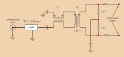
In actuality, there are more factors at play here. Looking at a typical ADC characterization board, it’s clear that most suppliers use permutations on a two-input transformer structure (Fig. 1). With the two 13.7-Ω resistors and the 1.41:1 turns ratio of T2, the circuit’s termination impedance referred to the input is very close to the desired 50 Ω when the ADC input resistance is placed in parallel with the 27.4 Ω of shunt impedance.
This structure is very useful in attaining a low driving impedance (12.5 Ω, in parallel with 13.7 Ω, equals 6.5 Ω on each side). However, it needs a higher input power level to reach full scale (FS). As such, combining the 3-dB pad, the transformer insertion losses, and the step-down for the 2-VPP-FS ADC requires 17 dBm (or 4.5 VPP) at the input.
The Real Secret
Although all of this effort achieves the desired 105-MHz input SNR for the ISLA216P25 ADC (up to 74.5 dBFS), it still requires one more super-critical bit of test hardware that’s seldom shown in evaluation board schematics. Figure 1’s passive interface is very broadband. Looking at the transformer specifications, it offers a −3-dB span of 10 MHz to more than 1 GHz. With such a wide analog bandwidth, the test circuit would integrate lots of noise at the input pins, which degrades SNR.
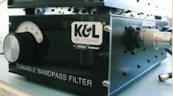
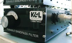
To avoid the noise problem, ADC manufacturers employ narrow bandpass filters ahead of the input (Fig. 2). This (expensive) tunable bandpass filter is extremely effective at constraining the spectrum at the input to the circuit in Figure 1. Thus, it delivers very low integrated noise and vanishingly small harmonic distortion terms for single-tone tests.
Tunable filters become vital components when trying to obtain the highest SNR datasheet numbers for a high-performance ADCs. However, it’s unrealistic to expect designers to include their equivalent in any real system. Also, these 5%-of-center-frequency narrow-width filters pass a narrow spectrum to these very high-clock-rate ADCs.
It’s acceptable to characterize the IC with a less than 5% bandpass-filtered test signal. Still, most real systems need to use a much larger portion of the available Nyquist band (FS/2). By using real filters with wider passbands, the integrated spot noise at the ADC input will be greater than that delivered during ADC characterization. The SNR achieved in production systems must be less than the ADC datasheet numbers.
Approaching “ADC-Only” Numbers
Another specification integral in optimizing ADC performance is SFDR in the FFT that processes the ADC’s raw output. The harmonic-distortion terms at the inputs of the ADC combine in-phase with the ADC-generated terms. For instance, if the lab-tested ADC generates a harmonic with amplitude of −85 dBc, and the input signal level also is −85 dBc, the FFT is expected to show −79 dBc.
To minimize SFDR degradation from the datasheet ADC-only tests (using the extremely clean signal coming out of the filters in Figure 2), the input distortion levels should probably be greater than −20 dBc below the rated ADC performance. Achieving super high linearity (i.e., low distortion) implies exceptionally high quiescent power in the final-stage amplifier and/or a very high loop gain in that stage for the intended frequency band of interest.
Such low harmonic distortion signals are only possible if the last stage amplifier has a bandwidth far wider than the desired signal band. As a result, a noise-power, bandwidth-limiting, inter-stage filter is required to reduce the SNR degradation introduced by that amplifiers’ broadband noise.
Final system performance, for the most part, comes down to the passive filter between the last amplifier and the ADC. Some design considerations must be applied:
- While the test circuit in Figure 1 added 7-dB insertion loss from the input to the ADC, it’s usually preferable to target 1.5- to 2.5-dB insertion-loss filters to keep the required voltage swing out of the last stage amplifier to a range only slightly higher than the intended ADC input range.
- Relatively low impedance values can limit the noise added by the resistors and present a low source impedance to the ADC.
- Conflicts arise when keeping the filter input impedance R to the amplifier outputs relatively high (to avoid unnecessary distortion degradation due to heavy loading of the last amplifier). Designers must also include the ADC input impedance as part of the filter-element design. Because these specs often have no specified tolerance, it’s best to include external elements that combine with the ADC terms so they dominate the value for the filter design.
- The passive filter elements should display reasonable tolerance. Mismatches in the series element values for differential filters will lead to converting some part of the output differential signal to common mode. (Also, if there’s a common-mode component to the output, it will get converted to differential.) This matching is intended for the series elements. Therefore, the differential capacitor elements often can exhibit 5% tolerance, while good results have been achieved using 1% resistor and 2% inductor tolerances.
There are obviously some tradeoffs, and the final design often becomes a bit empirical. For further insight, the ISLA112P50/55210EV1Z evaluation daughterboard offers a detailed example design. A 12-bit, 500-Msample/s ADC experienced only a 0.6-dB SNR degradation, while SFDR from −1 to −6 dBc (depending on the frequencies).


