This article is part of the TechXchange: PCB Tools and Technology
Members can download this article in PDF format.
In today’s designs, printed-circuit-board (PCB) real-estate comes at a premium. Fortunately, tiny components ranging from operational amplifiers (op amps) to temperature, Hall-effect, and millimeter-wave (mmWave) sensors can help you make the most of available space without compromising performance. You might face challenges, though, ranging from stringent isolation requirements to your company’s component second-sourcing policy. However, design strategies can be employed to overcome these hurdles and more.
Sponsored Resources:
- Second-sourcing options for small package amplifiers
- Achieve smaller isolation designs without compromising performance
- Driving industrial innovation with small-size sensors
Compact Sensors
Sensors have various roles to play in compact industrial applications. Maintaining an acceptable temperature range, for example, can be a critical factor in ensuring reliable and consistent system-hardware operation. Along those lines, Texas Instruments’ TMP390 temperature switch can autonomously assist in cooling or warming a system before its processor powers up, eliminating dependence on software. The TMP390 offers fully integrated dual-channel threshold monitoring and a built-in trip function while providing more than 60% area savings compared with an equivalent discrete implementation.
Hall-effect sensors have a role to play in compact brushless dc (BLDC) motor applications for healthcare and other products. TI’s DRV5011 Hall-effect latches (Fig. 1), for instance, enable the placement of three Hall-effect latches on a board to monitor speed, direction, and location for the commutation of a small BLDC motor in a handheld drill. For vacuum robots, two DRV5011 sensors can measure wheel speed and direction.
TI also supports autonomous industrial applications with a line of antenna-on-package (AoP) mmWave sensors that can process various types of data at speed to make real-time decisions, including sensing and responding to human activity. The mmWave sensors’ antenna configurations determine object-detection range, resolution, and maximum field of view. The AoP design, with the antenna integrated onto the device, saves the board space that would otherwise be allocated for a separate antenna.
Isolation Requirements
When designing for industrial applications, you might face significant challenges related to isolation. Your customers might want more functionality in a smaller package, but certification bodies like UL are not relaxing their minimum-dimension requirements for high-voltage creepage and clearance.
The challenges can be especially significant if you’re attempting an isolator design using discrete components, which could include a transformer, transformer driver, rectifier, and regulator. You may face creepage and clearance constraints for each high-voltage interface between components, which means that each component must meet the requirements of the relevant certification bodies.
As an alternative, you can replace the discrete solution with the TI ISOW7841, which integrates isolated data and power functions in a single package. The ISOW7841 requires just two decoupling capacitors and occupies a mere 33% of the board space needed for the discrete solution.
An approach based on the ISOW7841 offers benefits beyond PCB area savings. Board height is another advantage. The ISOW7841 is just 2.55 mm thick, vs. 4.1 mm for an external transformer required to implement a discrete version with the same functionality. In addition, TI obtains certification by agencies such as UL, VDE, CSA, and TÜV SÜD for all its isolators, with most certifications available within six months of device release. Finally, devices like the ISOW7841 offer simplicity, implementing thermal-shutdown, current-limiting, and soft-start features without additional components.
Second Sources
As you begin an industrial-design project, you’re likely to find an increasing number of small-package devices such as op amps that can be integrated into your project. What might be tough to find, however, is a pin-to-pin-compatible second source that you could turn to if your original supplier has trouble meeting demand.
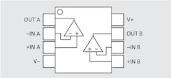
For example, if the design requires a component such as a dual op amp (Fig. 2), you might find one that comes in a small-outline no-lead (SON) or small-outline transistor (SOT) package. However, it’s possible that the only functional equivalent may only come in a small-outline integrated circuit (SOIC) package, thin-shrink small-outline package (TSSOP), or very-thin-shrink small-outline package (VSSOP).
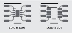
Fortunately, you can often modify your PCB layout to accommodate two package types, thereby ensuring that you have an alternate source. For example, you can lay out your PCB to accommodate an SOIC as well as either a SON or SOT package (Fig. 3). Other layout options can accommodate a TSSOP or SON, TSSOP or SOT, VSSOP or SON, or VSSOP or SOT.
When implementing layouts that can accommodate two package types, keep in mind two design and manufacturing considerations. First, take care to ensure adequate spacing between the pads of your preferred small-package device and the pads of your larger second-source device. A common PCB manufacturing design rule calls for at least four mils of space.
Second, note that the footprint of your larger second-source device may increase the trace lengths between the preferred small-package device and decoupling capacitors or other passive components that must be located near it. Take care during simulation or physical prototype evaluation to make sure these longer trace lengths don’t cause troublesome noise to couple into your SON or SOT device.
Conclusion
Compact temperature, Hall-effect, and mmWave sensors as well as isolators allow you to cram ever more functionality onto increasingly small PCBs for industrial and other applications. One possible challenge when choosing devices such as small op amps is the lack of a second source in your preferred SON or SOT package.
Fortunately, you can adapt your layout to accommodate functionally equivalent devices in larger packages. Although your PCB will be space-constrained by the larger package, the technique provides a simple way to ensure a second source while controlling costs, and it paves the way for future, even smaller versions of your design when SON or SOT second sources do become available.
Sponsored Resources:


