Members can download this article in PDF format.
Gallium-nitride (GaN) wide-bandgap (WBG) semiconductor devices enable higher power density and efficiency than do silicon metal-oxide-semiconductor field-effect transistors (MOSFETs) or insulated-gate bipolar transistors (IGBTs). They also offer advantages compared with WBG SiC devices for many applications. GaN-based components can achieve switching frequencies beyond 150 kHz in power-factor-correction (PFC) topologies and beyond 1 MHz in dc-dc power-converter applications.
Sponsored Resources:
- Make the Most of Your GaN Designs
- Is GaN reliable? Your key questions answered
- Optimizing high-voltage, high-power designs with GaN
Compact Magnetics
Texas Instruments offers a line of GaN FETs for applications ranging from consumer power adapters to electric-vehicle onboard chargers. When operating at frequencies higher than 500 kHz, the devices enable you to reduce the size of magnetic components up to 60% compared with other devices. In addition, TI’s proprietary GaN-on-silicon process yields GaN devices designed to keep high-voltage systems safe.
Some specific applications for these components include telecom and server power supplies—they let you reach the 80 PLUS Titanium-level energy-efficiency standard, providing 96.5% total energy efficiency and more than 100-W/in.3 power density. In addition, TI GaN devices can achieve 1.2-kW/l power densities for bidirectional ac-dc power-conversion systems used in solar and energy-storage applications.
GaN vs. SiC Details
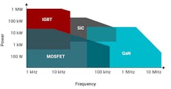
In addition to outperforming MOSFETs and IGBTs, GaN devices also offer advantages compared with WBG silicon-carbide (SiC) devices. SiC devices can attain higher power levels than GaN (Fig. 1) and operate at voltages as high as 1,200 V, making them a good fit for applications such as locomotive traction inverters. In contrast, GaN devices typically have 600-V ratings—however, they can switch at much higher frequencies and offer other advantages as well.
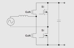
For example, in a totem-pole single-phase PFC configuration (Fig. 2), GaN devices exhibit zero reverse-recovery losses. In contrast, a SiC device can have greater than 85 nC of reverse-recovery charge.
In addition, a GaN device’s switching energy is more than 50% lower than that of a comparable SiC version, leading to a higher-efficiency PFC stage. Similarly, TI’s GaN devices, which include integrated gate drivers, offer fast switching speeds to 150 V/ns, resulting in an 82% reduction in losses compared with SiC FETs and 63% compared with discrete GaN FETs.
Furthermore, the availability of advanced driver features in TI’s GaN devices enables a reduction in dead-time losses of more than 67% compared with both SiC and discrete GaN implementations, without the need for complex firmware or hardware control.
TI GaN devices also will find homes in three-phase PFC topologies. The 480-V ac line-to-line voltages and 900-V and higher dc bus voltages typical of such applications exceed the ratings of individual GaN devices. However, multilevel topologies allow TI GaN devices to serve some higher-voltage three-phase applications. In these cases, TI’s devices offer better thermal distribution as well as higher system densities and efficiencies when compared with SiC devices or IGBTs (see table).
GaN devices also offer cost advantages compared with SiC. Several cost factors, including those associated with packaging and test, will be similar across technologies and needn’t be considered in a high-level comparison. Factors that do change between GaN and SiC include costs associated with the substrate, with fabrication, and with the number of chips per wafer.
Because GaN devices are grown on standard low-cost silicon substrates, manufacturers are able to leverage their existing equipment. In contrast, SiC can yield more chips per wafer, but it requires a special and expensive high-temperature manufacturing process with temperatures exceeding 2,500°C. Texas Instruments estimates that a GaN device can cost 1.3 times that of a similarly rated superjunction MOSFET, while a comparable SiC device would cost 2.4 times that of the MOSFET.
Reliability
Reliability is a key consideration for any semiconductor technology, and the power GaN industry has invested considerable effort to accelerate reliability development. Texas Instruments achieved reliable GaN devices through a comprehensive in-house reliability program and an embrace of industry-wide GaN standards, such as those promulgated by JEDEC’s JC-70 Wide Bandgap Power Electronic Conversion Semiconductors committee.
The committee has released GaN-specific guidelines including JEP173, describing a dynamic on-resistance test method; JEP180, covering switching reliability evaluation procedures; and JEP182, describing a test method for continuous switching evaluation. Other relevant standards that address extreme operation include IEC 61000-4-5, which covers surge immunity.
In addition, TI GaN parts for automotive applications are tested in accordance with AEC-Q100. Texas Instruments also has been active in the development of an industry-wide body of literature describing GaN failure mechanisms and their acceleration.
GaN-specific reliability efforts arose because traditional silicon qualification methodologies failed to fully address GaN issues. For example, Texas Instruments’ researchers noticed that hard-switched transitions could cause overheating in early GaN devices. Consequently, they developed a comprehensive approach to validate GaN reliability across a range of applications.
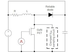
As part of this approach, they developed the test vehicle shown in Figure 3 to exercise potential failure mechanisms. The test vehicle can be used to provide accelerated hard-switching stress testing in accordance with JEP182, and it’s able to measure dynamic on-resistance in accordance with JEP173. The researchers concluded that TI GaN devices remain robust in both hard-switching and soft-switching applications.
To enhance system-level reliability, TI integrates overtemperature and overcurrent protection as well as undervoltage lockout into its GaN devices. The company packages its GaN devices using a low-inductance leadframe to minimize ringing, further improving reliability.
Conclusion
GaN devices offer improved power density and energy efficiency in a range of applications, including consumer dc-dc converters, electric-vehicle onboard chargers, telecom and server power supplies, and bidirectional ac-dc power-conversion systems used in solar and energy-storage applications. Texas Instruments offers a portfolio of GaN devices with integrated gate drivers and protective functions to ensure lifetime reliability and lower system costs versus competing solutions.
Sponsored Resources:


