Members can download this article in PDF format.
Around here we sit through many presentations about miniaturization of components and performance efficiencies realized at the same time. We also hear about the effort spent on reducing the size of passives used for energy conversion as inductors, capacitors, and transformers typically take up a large portion of the solution size.
Sponsored Resources:
- Are Thermals Keeping You Up at Night?
- 3 Ways to Overcome Thermals
- How to Achieve Greater Power Density
For engineers, all of this means more attention must be paid to thermal management and the junction temperature of semiconductor devices, which handle the conversion of power to a usable form. After all, when a device is running, it consumes electrical energy that’s transformed into heat. And if this heat isn’t properly controlled, it can negatively affect efficiency or even damage the board.
Simply shrinking a power supply, however, usually means you will be dealing with a challenging set of thermal issues. It becomes harder to obtain a sufficient surface area in contact with air that’s necessary to achieve effective heat dissipation.
On the plus side, shrinking systems and components leads to higher power density. Therefore, in addition to improving thermal resistances, if we can develop more efficient components and systems, power dissipation can be reduced. And that can directly result in lower temperatures.
Mitigating Heat Effectively from the IC Through the PCB
What stands in the way of achieving higher power density? Thermal performance has been one of the limiting factors. Proper circuit packaging is important for the heat to exit the system easily. This allows the system to avoid experiencing unwanted temperature rises.
Thermal performance is an electrical byproduct of power-management ICs, which you can’t ignore or eliminate via filtering components at the system level. The mitigation of thermals requires small adjustments throughout every step in the development process so that the design can achieve its system requirements for a given size constraint.
Let’s examine a few of Texas Instruments’ approaches to the problem. Most electronic systems have printed circuit boards (PCBs) with various components that dissipate power under different operating conditions. A bond-wire-type quad flat no-lead package (QFN) with an exposed pad is a popular package from a power density point of view.
Typical QFN packages are built using bond-wire interconnects between silicon and frame, which usually have very high electrical resistance. In a typical scenario, a QFN package with an exposed pad connected to the PCB results in more than 90% of power conducted from the package through the PCB to ambient air.
The HotRod QFN
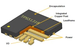
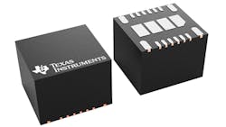
TI has developed a clever approach to improve package thermal performance to a degree beyond that of the previous generation. Called a HotRod package, it replaces QFNs with a flip-chip style package (Fig. 1). The electrical connections are made via lands on the bottom side of the component to the surface of the connecting substrate (PCB).
TI's HotRod interconnect distances it from all other packages with the silicon die flipped directly on a leadframe. This reduces the interconnect parasitics and lowers the dissipated power while still offering a large exposed pad for efficient heat transfer to the PCB through thermal vias (Fig. 2). Thus, it brings together the best of both package technologies for optimum performance.
HotRod QFNs are available in number of formats and sizes. The package is molded and mechanically singulated from a matrix of leadframes. PCB singulation is the process of separating multiple individual circuit board assemblies from the panel that they were assembled in. Package size is determined by the encapsulated die size and number of signal pins.
Greater Power Density in Server Power Supplies
Everything around us is becoming more data-hungry and data-driven. Consequently, power density is a must-have requirement for modern server power-supply units (PSUs). The latest generation of server PSUs are in the range of a 3-kW (250 A at 12 V) power rating.
To help meet ever-increasing power needs of servers and data centers, TI developed fully stackable 60- and 80-A eFuses. When selecting an eFuse, it’s important to have the highest current in the smallest size. By integrating a MOSFET, current monitor, comparator, active current sharing, and a temperature monitor, the TPS25985 and TPS25990 eFuses can significantly reduce the total PCB or printed-wiring-board area.
Server power systems operate at a wide ambient temperate range (–40 to 85ºC). Hot-swap controllers or eFuses experience even higher ambient temperatures. Therefore, the thermal performance of these devices becomes a concern when high currents are packed in small packages. The TPS25985 and TPS25990 eFuses alleviate this worry, with the ability to operate at a 125ºC junction temperature.
Partnering to Solve Thermal Issues
Other useful techniques in thermal management might recalibrate your expectations. These include using low-resistance thermal-interface materials between two mating surfaces, applying gap-filler pads for large gaps, using heat pipes to transfer heat from hard-to-reach spots, employing fans to create forced convection heat transfer, and utilizing cold plates to spread out heat.
One thing to consider is that while circuit boards can be cooled down in a variety of ways, designing with thermal issues in mind at the beginning can dramatically reduce heat-dissipation problems. Achieving more power in smaller spaces, and enhancing system functionality at reduced cost, are now possible using TI’s advanced process, packaging, and circuit-design technologies.
TI also offers design tools to help such as a PCB thermal calculator to understand the board area required for high-power dissipating components. This tool generates a quick estimate of the expected junction temperature based on the copper spreading area on the PCB.
Sponsored Resources:


