What you’ll learn:
- Why isolated flows negatively impact design schedule and PPA.
- Benefits of unified DFT, synthesis, and physical design flows.
- Physical implementation optimization methods for test compression and scan chains.
Modern system-on-chip (SoC) designs continue to expand in size and complexity to meet the computing requirements of applications such as artificial intelligence (AI), machine learning (ML), and the data center. This trend also has increased the design-for-test (DFT) logic added to the SoCs to minimize test cost and maximize test quality. Furthermore, SoCs designed to be deployed in safety-critical applications further broaden the test requirements to include in-system test.
The growing test logic in SoCs has a significant negative impact on their power, performance, area (PPA) and turnaround time, all while designers are being pushed to optimize PPA and shorten the design cycle due to today’s highly competitive environment. Thus, a new paradigm of physically aware DFT is required, where DFT implementation is fused with physical design implementation to achieve an optimal design PPA with quick turnaround time.
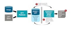
An example test flow illustrates the isolated DFT and physical implementation processes (Fig. 1). Such flows simply add DFT logic in the design and provide no guidance to the physical implementation process, later in the design flow, on the optimizations that can be performed.
During the physical implementation process, the tools are unaware of the DFT logic and analyze it similarly to other functional logic, resulting in a sub-optimal PPA for the entire design (functional plus DFT logic). Another major drawback of disjointed test flows is that they often lead to an iterative process between DFT and physical implementation to achieve design convergence through design change with re-synthesis or engineering-change-order (ECO) process, causing delays in development schedules.
Physically Aware Scan Synthesis
The benefits of physically aware scan synthesis on design implementation are well-known—it’s been a standard industry practice for almost two decades. For advanced designs, the growing test logic includes test compression, memory test and repair, in-system test and debug, high-speed TAP, clock controllers, IEEE 1500, 1687 logic, and so on. Hence, a similar physically aware implementation methodology that applies targeted optimizations to all test logic is needed to achieve the best PPA for the entire design.
That goal is typically accomplished by applying two important techniques:
- Enhancing DFT implementation infrastructure to help with logical and physical optimizations.
- Enabling synthesis and physical design processes to perform targeted optimizations of DFT logic.
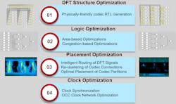
A flow for codec implementation and its scan-chain connections is based on these techniques (Fig. 2).
Physically Aware Implementation
In step 1, DFT Structure Optimization, the codec is split into multiple partitions to avoid the routing congestion that results from convergence of signals and scan chains to one monolithic codec location. In step 2, Logic Optimization, as the synthesis engine is aware of functional intent and the RTL structure of the codec logic, it performs targeted area, delay, and congestion optimization by balancing the local and global sharing of the codec logic’s signals.
During physically aware scan synthesis after the Logic Optimization phase, the scan chains are clustered into groups based on initial physical information and number of codec partitions. In step 3, Placement Optimization, the physical design engine is aware of codec partitions and performs congestion aware placement and routing of partitions and internal test signals needed for the codec. In addition, the scan-chain group connections to codec partitions are re-clustered to improve routing and wire length.
In step 4, clock path optimizations are performed by physically aware placement of on-chip clocking (OCC) and test clock routing for improved timing.
The optimizations shown in Figure 2 require DFT, synthesis, and physical design processes to work concurrently to form one seamless physically aware DFT implementation flow (Fig. 3).
PPA Results After Implementation
The PPA improvement percentages with such a flow on several industry designs are shown in the table.
Every design observed an improved design PPA with the flow that performed targeted optimizations only on codec implementation and its scan-chain connections. Similar techniques are being developed for other test logic such as MBIST, logic BIST, etc., and silicon-lifecycle-management (SLM) structures like path monitors and power-voltage-temperature (PVT) sensors, which would further enhance these metrics.
DFT is no longer a second thought during the design process as more test logic is needed to meet the test goals of today’s advanced designs. As the industry moves toward the integration of test flows with SLM capabilities, the isolated DFT and physical implementation technologies would either be unable to mitigate the negative impact of these structures on designs’ PPA or would require enormous efforts.
Designers must adopt advanced test technologies that are based on physically aware implementation and apply targeted optimizations to keep up with ever-expanding PPA and accelerated design-cycle requirements.


