This file type includes high-resolution graphics and schematics when applicable.
In one current design project, I’m working on an application that requires force sensing with a moderately high dynamic range, but not necessarily high absolute accuracy. That is, I need to be able to see small changes in a fairly large force, but I don't need tight absolute accuracy of the total force measurement. I need to look for changes on the scale of hours or days, so simply ac-coupling is not an option. The fancy strain-gauge units are out of the question due to cost sensitivity of the product, so I looked into force-sensing resistors.
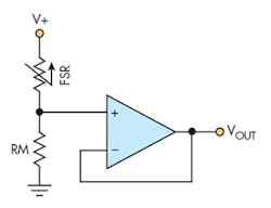
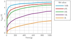
Interlink’s FSR400 series looks like a good fit, so I downloaded the datasheet.1 I immediately gagged on the recommended signal conditioning and resulting graphs shown at the bottom of page 3, duplicated here as Figures 1 and 2.
Stepping back to think this through, I note that a force-sensing resistor (FSR) starts at zero force with no (or at least very few) connections between conduction channels. As force is applied, more and more resistive channels progressively make contact, and they are electrically in parallel. Thus, resistance is inversely proportional to force, which is another way to say that conductivity is directly proportional to force. We could certainly use a piecewise linear curve fit to linearize this rather ugly transfer function, but aesthetics aside, resolution at the high end suffers terribly.
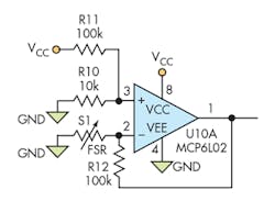
Because we can see that the FSR is actually converting applied force to conductivity (as opposed to resistance) in a more-or-less linear fashion, we can easily adjust our signal conditioning to yield a voltage that’s directly proportional to force, which then translates to an ADC output that’s linear in force. While it’s easy to use a bipolar power supply to make this work, most of my designs use only a single supply rail and rail-to-rail op amps, so my first attempt looked like Figure 3.
Initial Design with FSR
Presuming that U10 is an ideal op amp, there’s essentially no current into or out of the inputs. Thus, the noninverting (+) input is fixed at VCC/11 all of the time. Assuming VCC is 3.3 V, then, the input is at 300 mV. As long as the op amp isn’t in saturation, the inverting (–) input is also at 300 mV. Consequently, FSR S1 sees a constant 300 mV, and the current through it is directly proportional to applied force. Since that current can only come through R12, the voltage at the output is 300 mV plus an amount proportional to force, current times the 100K of R12.
For the FSR400, with zero applied force, the op-amp output is 300 mV. At approximately 180 gram-force, with an FSR resistance of 10K, the op-amp output is 3.3 V. Thus, we have a linear 3-V swing for 180 gram-force. If we then measure that output with a 12-bit ADC scaled to the full range from GND to VCC, we have a resolution of approximately 48.3 milligram-force per count.
We can adjust this full-scale range quite handily just by adjusting the voltage at the op amp’s noninverting input in any of a few dozen ways. I like to take advantage of the fact that microcontroller pins are quite flexible in their configuration, if you can get past thinking of just an input or an output.
Obviously, a typical microcontroller pin can be configured as an output and driven low, or an output and driven high. But what if we configure that pin as an analog input? Now it becomes, to the outside world, essentially an open, neither sourcing nor sinking current. Making it a digital input in theory does the same, but most parts will “consume out-of-spec current” with a voltage other than a pure high or low on a digital input.
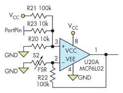
Modification with Selectable Force Ranges
So let’s modify Figure 3 to create Figure 4, which has three selectable ranges for total force. The selected resistor values, of course, determine the actual ranges. But for these simple selections, it works like this: If we set PortPin to be an analog input, there’s negligible current through R23, and we have the case of Figure 1, with a full-scale range of 180 gram-force. If we set PortPin to be a digital output and drive it low, the voltage at the op-amp inputs is now 157 mV. Zero force results in 157 mV at the output, while it takes approximately 400 gram-force to conduct sufficient current to drive the output to 3.3 V. Thus, we have 400 gram-force corresponding to a voltage swing of 3.143 V. On a 12-bit ADC, we span 3900 counts for 400 gram-force, or 102.5 milligram-force per ADC count.
Note here that modern microcontrollers approach the ideal in terms of I/O behavior surprisingly closely, especially to those of us who cut our teeth back in the bipolar days. The outputs are direct FET drivers, and at low current they get very close to the supply rail.
Input impedance is a tricky issue. Input resistance is typically very high, as you’re just looking into a couple of FET gates plus whatever leakage is offered by any clamp diodes that might be present. However, reactance can be fairly low, especially on ADC inputs, because a deliberate sampling capacitor is usually involved.
Manufacturers often try to simplify things for the pure-digital boys by suggesting a low-impedance drive, but all that’s really needed on a high-resistance source is a good-sized (and non-leaky!) capacitor. I often use either 0.1- or 1-µF ceramic for this purpose—it’s enough to absolutely swamp the typical 25-pF sampling capacitor that causes the “impedance” rating to be low. We’re going to take advantage of this nearly ideal pin behavior throughout the approaches presented here.
Above we saw how to increase the input range, at the expense of coarser resolution. Going the other direction, to a smaller range and finer resolution, we can drive PortPin high (VCC). Now the op-amp inputs sit at 1729 mV, and current through the FSR is proportionally higher. Full scale is approximately 27 gram-force. Even though we compressed the ADC into the top half of its range (because the “zero” is now at 1729 mV), our resolution has still improved greatly, to approximately 13.8 milligram-force per count.
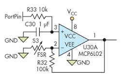
A Smaller, Finer Approach
But why can't we have our cake and eat it, too? Figure 5 assumes that PortPin is a pulse-width-modulated (PWM) output, which is typically available on one or even several pins of a microcontroller. If we drive PortPin at a reasonable frequency (a few kilohertz to a few hundred kilohertz), R33 works with C30 to form a low-pass filter. The op-amp inputs see a constant voltage that’s some fraction of VCC, as set by the duty cycle of the PWM output. Now we can adjust the voltage across the FSR anywhere from GND to VCC.
The case for GND is more important than is first apparent, too. In a very low-power system, where measurements are needed at relatively long intervals, setting PortPin low (Gnd) completely turns off the current through the FSR. This is an important consideration in my present application.
The purist in me still bristles at the loss of part of the usable range of the ADC, though. Certain microcontrollers in Microchip’s lineup can accept an external voltage for the more negative ADC reference voltage, compressing the ADC working range into the actual usable output range of the op amp. That is, I could use the reference voltage at the +input of the op amp as the more negative ADC reference, with VCC as the more positive reference. Therefore, the ADC full-scale range exactly covers the possible range of op-amp outputs. However, the accuracy spec suffers. If I could instead use a bipolar arrangement, with the far end of the sensor at a negative voltage and the ADC inputs always at GND, I could have the best of all worlds.
Optimizing MCU Pin Flexibility
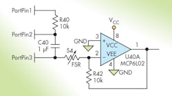
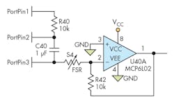
Pondering on this problem while mowing the leaves into windrows (it’s Fall here in Ohio as I’m writing this), I came up with a better way. Figure 6 takes full advantage of the flexibility of microcontroller port pins, with due regard for the minor non-ideal behaviors noted above. Here, PortPin1 is a conventional digital pin, configured as an output and set low as we begin. PortPin2 can be configured on-the-fly as either a digital output or an analog input. PortPin3 is a digital pin, sometimes an output and sometimes an input. The op-amp output goes to a pin that’s configured only as an analog input to measure the result.
In this configuration, the op-amp inputs stay solidly at GND unless the output saturates. Therefore, this configuration requires an op amp whose common-mode input range includes its most-negative supply rail and a smidgen below, as does the depicted MCP6L02.
To take a measurement, we assume C40 starts out discharged. We configure PortPin1 as a digital output, PortPin2 as an analog input, and PortPin3 as a digital output. Leaving both output pins set low during the idle time between readings minimizes idling power consumption and ensures C40 starts out discharged. We compute the time required to charge C40 to approximately 300 mV, and set PortPin1 high for that duration; then set PortPin1 to an analog input so no further current flows in or out there. Now we can measure the voltage at analog PortPin2 to determine the exact voltage on C40.
Next we configure PortPin3 as an analog input so that it will no longer source or sink current, and set PortPin2 as an output and low. The bottom of C40 is now 300 mV (or whatever actual voltage we measured) below GND. Note that we don't want to go more negative than 300 mV due to limitations of the microcontroller port pins. The end result is that the op amp’s output voltage is exactly proportional to the conductivity of S4, and spans the full ADC range.
If we know the values of R40 and C40 precisely, we can use a predetermined time to charge C40 to a known value. However, capacitors with better than 10% tolerance get quite pricey; hence, the ADC is used to measure the actual resulting voltage. We can then choose to either use the actual voltage achieved to compute the scaling of the output value, or “bump” the voltage up or down by driving PortPin1 high or low for short intervals until we achieve the desired voltage. By measuring the actual voltage on the capacitor, we can completely eliminate the tolerances of R40 and C40 from the measurement uncertainty.
If the above measurement results in a railed output, with the op-amp output driven full-scale high, then we’re on the wrong range. We can easily change the measurement range by using a lower voltage on C40 for a retry of the measurement. Halving the voltage on C40 doubles the available force measurement range.
If droop in the C40 voltage during the measurement turns out to be an issue, we can closely approximate its actual voltage during the measurement. After the output measurement, we simply revert the configuration of PortPin2 to an analog input, and PortPin3 to a digital (low) output, and measure the C40 voltage again after our weight measurement. Averaging the “before” and “after” measurements, possibly with unequal weighting, then yields a very good approximation to the actual voltage during the weight measurement.
With the measurement method of Figure 6, we eliminated component tolerances (other than R42) from the scaling of the measurement; utilized the full ADC range for maximum resolution; provided for multiple measurement ranges; and allowed the circuit to essentially power down between measurements. Total parts cost in volume is a few pennies, which is trivial relative to the cost of the FSR itself.
This circuit offers a great illustration of how straddling the fence between hardware and firmware can yield the optimum final result. Just a little bit of firmware combined with very simple hardware yields a precision measuring system with a large dynamic range.
Reference:
1. Interlink FSR400 series datasheet
Steven P. Hendrix, P.E., CFIAI is a Professional Engineer in Ohio, and has operated Hx Engineering LLC as a full-time, full-service design shop for 23 years. He holds a Bachelor’s in Computer Science and in Mathematics from the USAF Academy and flew for the USAF for six years before getting married to Kathy, starting a family, and starting Hx Engineering LLC. He can be contacted at [email protected], or at (330) 467-6301. Hx Engineering is located at 8660 Brandywine, Sagamore Hills, OH 44067-2818.
