Members can download this article in PDF format.
In designing an input stage for an analog-to-digital converter (ADC), engineers choose a particular amplifier, assign a target gain, and note the transducer or sensor input impedance to be matched. The task then is to reduce the output noise and distortion without incurring a large cost and power consumption penalty.
The design process described here explains how to ac-couple the signal path by pairing a low-noise, wideband, voltage feedback amplifier (VFA) with an input transformer. When the signal frequencies are well below loop gain crossover for the design chosen, this approach can provide much lower power consumption than an approach using standard RF gain blocks.
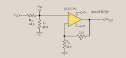
Four circuits are considered, but for the sake of space, only three are depicted as schematics. Hypothetical circuit 1 employs RF gain blocks between the signal source and subsequent signal process is not considered here. Figure 1 is the simplest op amp based gain stage with a 50-Ω input match.
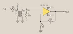
Circuit 2 employs transformer coupling with the signal applied to the non-inverting input of the op amp (Fig. 2).
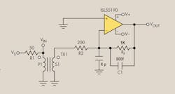
Circuit 3 uses transformer coupling and applies the signal to the op amp’s inverting input (Fig. 3).1
Noise Figure And Spurious Free Dynamic Range
Matching source impedances to amplifier input impedances using resistors is a common design practice. But there are multiple ways of doing this that have different effects on performance, depending on the topology employed.
Analysis of these effects requires an understanding of noise figure (NF) and spurious-free dynamic range (SFDR). NF indicates the sensitivity of a mixed-signal circuit. SFDR indicates the input amplitude range the circuit can handle.
The NF, expressed in dB, of any device is a measure of its effect on signal-to-noise ratio (SNR). That is, NF = 10 log(SNRIn/SNROut). Because there will always be a degradation in SNR going through a device, SNR and NF are always greater than 1. More precisely, NF is the ratio of the total output noise power of a device to the amplified noise power delivered to the input by some source impedance (usually 50 Ω).
In an ADC signal chain, SFDR is an indicator of the signal chain’s ability to handle very large and very small input-signal amplitudes. In the frequency domain, SFDR usually relates to the circuit’s response to a single-frequency or 2-tone sinusoidal inputs.
The characteristic is defined as the ratio of the RMS value of the carrier frequency at the input of the ADC to the RMS value of the next largest Fourier component of the output. This is usually the second or third harmonic-distortion (HD) term, but not always.
SFDR results can be stated in dBc (dB relative to the carrier-frequency amplitude) or in dBFS (relative to the ADC’s full-scale range). Depending on how the measurement is made, SFDR specs may be given in terms of a pre-defined frequency window or from dc up to the Nyquist frequency (half the ADC’s sampling rate).
Managing Noise Figure
Equation 1 defines NF in dB where everything is in powers (or voltage gains and voltage noise terms squared):
There are several typical simplifications to this equation, but given the noise of source impedance of RS (50 Ω will be used in these examples) delivered to an input having a total input referred noise power of Ni, the noise figure expression becomes Equation 2 (where a value of kT = 4 x 10–21 J may be used):
A useful reference point is that 1-nV/√Hz total input spot noise corresponds to an NF of 7.8 dB. Often, if the input match is being set resistively, the “1+” in the NF expression changes to a “2+,” meaning the 1-nV input voltage noise equates to an NF of 8.45 dB.
Reasons For Using Transformer Input
A simple expression for the input NF may be derived, starting from a simple noninverting gain amplifier (Fig. 1), with an input resistor to ground at its V+ input providing the input match, and the feedback resistor value chosen to provide a balance between the noise it might be adding versus parasitic loading effects.
With very low-input-noise op amps, such as the ISL55190, which offers 1.06-nV/√Hz voltage noise and 5-pA/√Hz current noise terms on each input, the contribution from resistor noise can add meaningfully to the total output noise. At these 1-nV/√Hz op-amp noise voltage levels, every tenth of a nanovolt of input-referred noise improvement is hard to come by.
This is where the transformer input options start to offer some paths to improvement. Equation 3 provides the NF1 for a simple, non-inverting design with a resistor to ground as in Figure 1 (matched in these examples to a 50-Ω source):
The “2” arises from achieving the match with a physical resistor. The numerator of the fraction represents the total input referred noise power of all the op-amp terms, while the denominator represents the noise power delivered to the input from the source resistor, RS, to a matched physical termination resistor equal to RS.
The only option for the circuit designer here, given any particular op amp, would be the target non-inverting gain and the Rf value. For example, using Rf = 332 Ω to avoid degrading the noise, but without excessive feedback loading, and targeting a gain of 10 V/V will provide a noise figure, NF1 = 10.23 dB, using the ISL55190 with only a 50-Ω input termination running noninverting (using eq. 3).
Bandwidth Issues
The second dynamic range issue a circuit designer should consider is the resulting bandwidth and loop gain for the design options. The non-unity gain stable ISL55190 offers a 1150-MHz gain bandwidth product, drawing 16 mA in single +5-V designs with rail-to-rail output and negative-rail input.
In this simple gain = 10 V/V example, that configuration should provide a closed-loop bandwidth of about 115 MHz. In a case like this, seeking a design for low output distortion up to the F–3dB point usually isn’t a good idea, as, by definition, the loop gain would have rolled off to 0 dB at that point.
Adding A Transformer
To compare the dynamic range benefits of adding an input transformer, perhaps backing off to 12-dB loop gain (at 0.25 times the frequency at which the loop gain = 0 dB) will provide a point of comparison. In this simple (no transformer input) design of Figure 1, more than 12-dB loop gain will be available up to 29 MHz. The gain would be 10 V/V from the matched 50-Ω input to the output (i.e., 20-dB gain).
Now add a step-up transformer at the non-inverting input (Fig. 2). With a turns ratio of “n,” an input match to RS still can be delivered if the resistor to ground on the V+ node is increased to n2Rs.
The transformer needs 200 Ω at the V+ input to ground to transform impedances as well as voltages. The tradeoff is a noiseless voltage gain at the cost of increased source-impedance gain for the non-inverting input-current noise. Equation 4 shows the NF2 expression for this approach:
The total input referred noise for the combined transformer plus op amp shows the op-amp voltage noise divided by the turns ratio and the current noise term multiplied by “n” (Eq. 4). The term en in the equation represents all the terms in the numerator of Equation 3 except the Ini term. From this, an optimum turns ratio that will minimize NF2 can be derived as:
Picking an actual transformer with an integral turns ratio, say 2, allows the op-amp gain to be reduced to 5 and still hit the same overall gain target of 10 V/V. Using the ISL55190 datasheet values in the equation will show a significant improvement: NF2 = 6.98 dB.
For the same overall gain, then, what has happened to the usable frequency span—the frequency range before the loop gain drops below 12 dB?
Decreasing the amplifier gain to 5 V/V has, of course, expanded the nominal F–3dB to 230 MHz, with a loop gain greater than 12 dB up through 58 MHz. This has at least doubled the useful frequency range, simply by splitting the gain between the transformer (gain of 2), and the amplifier (gain of 5), while also reducing the apparent input-referred noise. Since the achieved gain is still 10 V/V, by definition, it also has reduced the output spot noise.
Driving The Inverting Input
A more interesting result may be achieved by bringing a transformer-coupled input into the inverting terminal of the op-amp input (Fig. 3). The transformer in the circuit retains the 1:2 turns ratio, but now R2 is both the gain and termination impedance. The V– node of the op amp is at virtual ground, so R2 = 200 Ω will both input-refer to look like 50 Ω on the input side of the 1:2 turns ratio transformer and combine with the 1-kΩ feedback resistance to provide a signal gain of –5 V/V.
Now, on the V+ node, there is no resistor or noninverting-input bias-current noise. But even more usefully, consider the reduction in gain for the op amp’s input voltage noise to the output.
Looking at the noninverting gain, the output sees both the R2 + n2RS (actually 2*R2) as a gain element. Thus, the noise gain has been reduced to 3.5 V/V, while the signal gain is now –10 V/V overall. If the signal inversion is an issue, the transformer can be connected to invert, providing a net noninverting path. Equation 6 provides NF3 for this configuration:
In the equation, Av– = Rf/R2 in Figure 3 and the ii term is the inverting current noise. (Use only gain magnitudes in the NF equations.) This expression can also lead to an optimum turns ratio equation:
One drawback to this approach is that the Rf is now completely constrained by the RS, turns ratio, and target gain, which is why it no longer shows up in Equation 6. Putting in the ISL55190 characteristics for the “n” = 2 target gain of –10 V/V gives an NF3 of 6.99 dB—basically identical in this case to putting the transformer on the V+ node. The 3.5-V/V noise gain should extend the frequency before the loop gain drops to zero out to 328 MHz, providing a loop gain greater than 12 dB through 82 MHz. This relatively low noise gain for the decompensated ISL55190 is compensated by the 0.8pF feedback and 4pF capacitor ground on the inverting node in Figure 3 (ref. 1).
Comparing Design Options
The table summarizes the three design options that have been discussed here: direct coupled non-inverting, transformer coupled using the non-inverting op-amp input, and transformer coupled using the inverting input. For the two transformer-input options, the input-referred noise from RS at the termination point has dropped from 1.4 nV/√Hz (solving Equation 2 for Ni) for the simple noninverting op-amp case, to 1.03 nV/√Hz, while the frequency span of usable loop gain has been extended using the 1:2 transformer step up. The transformer consumes no power. Combined with an already very low-noise device, this yields a significant improvement in dynamic range.
Using a free simulation tool for the Intersil op amps, iSim PE, and a good model for the ADT4-1WT transformer (1:2 turns ratio), a comparison of the simulated F–3dB may be made for each of the three circuits considered here. Those results are shown in the table where, as expected, the bandwidth extends quite a bit from the simple noninverting circuit. The inverting design is being bandlimited a bit due to the compensation capacitors, but is very stable.
Even though the inverting design of Circuit 3 seems to be more band-limited, it will still be providing a higher loop gain at the lower frequencies, improving distortion over Circuit 2. Going to a noise gain of 3.5 from a gain of 5 will increase the loop gain by 3 dB.
Where very low power, low noise, and distortion wideband stages are required, circuit designers should consider adding a step up transformer to the op amp’s input to get an improved dynamic range solution. Use the NF equations shown here to compare the approaches, and then check the final response shape using vendor simulation tools.
Application To Differential Signal Paths
While these circuits have been single-ended I/O, the transformer coupled options using either the noninverting option or the inverting input option can be implemented differentially. The transformer also can be used as a differential output, so it is a very simple matter to connect into differential versions of these circuits using a dual version of the op amp, such as the ISL55290.
For inverting mode implementations, these techniques are also very suitable to fully differential amplifiers (FDAs) like the ISL55210. In this case, the VFA design is preferred since the feedback resistor value is completely set by the impedances and gain targets, and it is helpful to have considerable flexibility. Current feedback-based FDA devices have a strong dependence on dynamic characteristic with the value of the feedback resistor. They can provide very high full-power bandwidth, if the Rf used is close to the recommended value.
This article was originally published on 3/22/12.


