What you’ll learn:
- How an acoustic micro imaging tool is more effective in collecting echoes.
- What is Virtual Rescanning Mode (VRM)?
- Examples of how VRM works with matrix files of flip chips.
When a component fails in service, the failure may do structural damage that obliterates any possible clue about the cause of the failure. Acoustic micro imaging tools may help solve this problem in advance.
When ultrasound is pulsed into a solid material, it travels at a predictable speed through the material until it encounters the interface with a second material. Here, a portion of the pulse crosses the interface, while another portion produces echoes that fly back to the transducer that launched the ultrasound, as well as in many other possible directions. There are innumerable echoes and they may differ from each other in their amplitude, their acoustic frequency, their arrival time at the transducer that launched them, and their polarity.
To image the interior of electronic components non-destructively, the ultrasound-pulsing transducer of an acoustic micro imaging tool moves just above the component’s surface. Tens of thousands of times per second, it launches a pulse into a given x-y location, collects the return echoes from the depth or depths of interest, and moves on to the next location. The return echoes from each x-y location determine one pixel in the acoustic image.
If large numbers of components are being screened to determine their fitness for assembly, only those echoes coming from the depths where defects most frequently occur will be collected to make acoustic images. The majority of defects contain air; thus, they’re easily imaged because a solid-to-air interface reflects nearly all of the ultrasound that strikes it and is a strong signal.
Echo Generation and Collection
In a flip chip, voids or delaminations in the underfill near the solder bumps and the bump bonds are risky. In a BGA, defects above or below the die pose a risk. In a multilayer ceramic chip capacitor, any air gap between layers at any depth can cause trouble. To remove defective components from assembly, automated acoustic imaging typically collects echoes from the depths where the expected defect types are most likely to occur.
Each component can generate far more echoes than may be used for routine screening. But all of those echoes are able to be used for a less-frequently performed but highly useful purpose: A post-mortem on a failed component, even when the physical component is orbiting the moon or otherwise unavailable.
VRM and the Matrix
The imaging mode is termed the Virtual Rescanning Mode (VRM) by Nordson SONOSCAN, its developer and maker. It’s used on C-SAM tools to scan individual components that will be employed in very critical applications.
Utilizing an ultrasonic transducer that will penetrate deeply enough to image the whole meaningful volume of the component, the module simply collects and stores every single echo waveform along with its precise location. The data from scanning of an individual component is stored in a very large “matrix” file in case it’s needed.
Many matrix files are never used. Only when the component has failed in its critical role is the matrix file examined to see what clues it may offer about the cause of the failure (Fig. 1). Matrix files are typically made only for components that are going into high-end applications, where failure has significant consequences.
The matrix file can be used to essentially re-image the component as though it were the original, intact physical component. It has all of the raw echo data reflected by all internal material interfaces at all x-y locations. The physical component may have been imaged by only one or a few of the 15 or so imaging modes that have been developed for C-SAM tools, and some of its depths may have been ignored.
In the matrix file, all of the depths can be imaged, and in any feasible imaging mode. The virtual component can, for example, be non-destructively cross-sectioned along a line having any orientation. It may be imaged in simultaneous very thin slices, or in three dimensions, or in any of the other imaging modes. Any structural features, including defects, will be imaged.
New users of VRM are sometimes surprised that the VRM image is identical to an image of the physical component using the same imaging parameters. But the matrix file simply contains all echoes from the component. The matrix echo collection contains, intact and unchanged, all echoes used in the original screening of the component, plus a great many more.
Echoes from original imaging or in the matrix file both carry the same types of information about each x-y location on an interface—its depth, the amplitude of the echo, the frequency range of the echo, and the polarity (positive or negative) of the echo. This means, among other things, that an echo having a frequency content range from 70 to 120 MHz can be imaged separately at each frequency from 88 to 91 MHz, for example, or 92 to 95 MHz.
That imaging mode is known FFT (fast Fourier transform), or simply as the “frequency mode.” Close work with a matrix file using this mode or one of the other modes can answer many post-failure questions.
Flip-Chip Matrix Examples
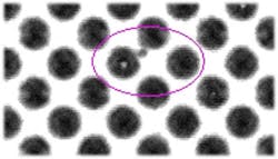
Figure 2 was made from the matrix file of a flip chip that later failed in service. A likely cause of failure is the air bubble amid the circled group of solder bumps. The most likely scenario is that the air gradually permitted portions of one or both of the adjacent solder bumps to flow into the bubble until they met. The resulting short circuit would cause a malfunction in the flip chip and therefore a malfunction in the system.
One small additional note: The solder bump in the left side of the oval has a bright spot near its center. The air bubble between the two solder bumps appears black because the small area at its top surface that reflects over 99% of the ultrasound is too small to be imaged. However, the apparent air bubble on the bump to the left may be flattened and thus have a larger area to reflect ultrasound.
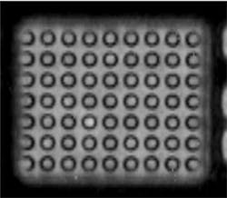
Figure 3 is a VRM image made from the matrix file of another flip chip. This flip chip had failed during testing. A probable cause is the somewhat brighter solder bump just to the left of and below the center of the image. It’s somewhat brighter tone contrasts with the other bumps, all of which are essentially the same color. The affected bump doesn’t reveal much fine detail, but it’s likely that the air causing the bright reflection eventually severed the electrical contact and precipitated the failure.
Both examples illustrated here are flip chips, but any imageable component can take advantage of VRM. For example, multilayer ceramic chip capacitors going into critical applications aren’t expensive, but they’re worth imaging because even a small air gap can expand until it forms a conductive pathway linking two electrode layers.
Not Just Air Gaps
The agents of potential failure aren’t always air gaps, though. A plastic IC package, for instance, may pass routine automated inspection because it has no gap-type features. However, after failure, the VRM images may find no air gaps, but a tilted die that would, among other things, put pressure on wires and cause disconnects.
The tilted die can be found by using the matrix file to generate a small or large number of sequential, vertically thin images. Viewed in order, they will display the part of the die that’s momentarily in focus slowly travel from the top-most corner of the die to the bottom.
VRM is the answer to engineers who have often thought, after a significant component failure, “I wish we had the component here right now, in its original condition, to look for truly hidden structural anomalies.” With proper planning, VRM fulfills this wish.


