A lack of planarity along the interface between the solder and the ceramic raft in an IGBT module is a common anomaly that can make heat dissipation uneven across the die and cause the die to crack. Deviations from planarity in both the raft and the solder are typically slight, with variations typically measured in tens of microns.
These deviations from planarity can be imaged by a number of acoustic micro imaging modes. However, the mode that makes it easiest to visualize a particular module’s irregularities and the opportunities for mischief that it may present is three-dimensional acoustic micro imaging, or 3D-AMI.
How does an instrument such as the Sonoscan C-SAM tool, which pulses ultrasound into a sample and collects return echoes, produce a three-dimensional image? The IGBT module is positioned above the transducer that, along with its accompanying “Waterplume,” is inverted. In this position it can scan the bottom-side base plate of the module. Ultrasound at these frequencies (30 MHz, for example) won’t travel through air, so the Waterplume keeps the transducer constantly coupled to the baseplate as the two scan back and forth.
Each second the transducer launches several thousand pulses of ultrasound into the baseplate. As the sound travels into the IGBT module, it’s partly reflected by interfaces between materials. The first interface is that between the water and the baseplate. The second is between the baseplate and the solder. Both of these interfaces are typically planar.
Echoes reflected by the water-baseplate interface will all arrive at the transducer for collection after the same number of nanoseconds. Those reflected by the solder-to-raft interface, however, will arrive at the transducer after a uniform interval only if the raft is planar. If it’s warped or otherwise distorted, they will arrive at various times.
Both going to and returning from an interface, ultrasound travels at a speed determined by the material it’s traveling through. Through solder, it travels at about 4000 meters per second. Because each pulse-echo sequence takes only a few microseconds, the fast-moving transducer can carry out thousands of sequences, and collect thousands of echoes from individual x-y locations, per second.
The transducer can detect four properties of an incoming echo: its ultrasonic frequency spectrum, its amplitude, its polarity, and its arrival time. For 3D imaging, the transducer depends on the arrival time, or more precisely, the time required for the echo to travel from the solder-to-raft material interface to the interface with the baseplate at the top of the solder. Time is converted into distance, and each echo becomes one pixel in the acoustic image.
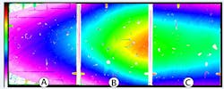
Figure 1 is the acoustic image of the solder-to-raft interface in a module where the three rafts are all badly distorted. This is a Time Difference mode image, in which arriving echoes are assigned pixel colors according to their depth. Although it differentiates depths, this isn’t a 3D image because the pixels haven’t been converted into vertical lines.
1. Viewed through the baseplate, two-dimensional colors identify local depth of the solder-to-raft interface.
The view in Fig. 1 is through the planar baseplate. The solder is thickest, and the raft-to-solder interface deepest, in the red area at the right of the center raft. The vertical color map at left displays the whole sequence of colors: yellow solder is thinner than red, blue is even thinner, etc. The varying thickness of the solder is caused by the distortion of the raft. The thousands of echoes used to make this image were originated from various levels within a depth ranging from the baseplate-solder interface to the anticipated solder-to-raft interface.
Creating the Acoustic Image
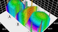
To produce an acoustic image displaying the dimensions directly, software first identifies the distance of each echo’s point of origin above the baseplate and assigns a color for that distance. The vertical distance of all pixels is then exaggerated by a given amount. The resulting 3D structure must be tilted off of its vertical axis to make all three dimensions visible.
In Fig. 2, the pixel data has been elevated to display all three dimensions, and the module has been tilted. The white area is the baseplate, which was at the top in Fig. 1, so the various depressed contours of the raft-to-solder interfaces are now on top and appear as domes. The highest point on the center raft, which was red in Fig. 1, is also red here. It’s the farthest from the white baseplate and thus represents the deepest depression in that raft. The other two rafts both have more gently rounded depressions; these two rafts are moderately dished.
2. Three-dimensional view of the same three solder-to-raft interfaces.
The tall thin spikes are simply locations where the solder at the edge of a raft rises above the level of the raft. The vertical dimensions of these bumps are exaggerated along with the solder-raft interface, and the solder typically rises only slightly above the raft.
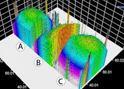
In Fig. 3, the image of the module has been rotated to view the features from the side. The multi-colored flat walls on the near sides of the rafts simply use the color of the pixel directly above. This can be seeing raft B, where part of the sloping surface is at the dark blue depth; on the flat side facing the viewer, dark blue lines from this depth simply extend straight down. The vertical dimensions are of course magnified, but the proportions have been preserved. The middle raft actually has at its left side about one-fifth the thickness of solder that it has at its right side. The scale at the bottom the image indicates that the width of the group of rafts is about 100 mm.
3. Side view of the same rafts.
Raft Discrepancy
There’s an apparent discrepancy in the structure of raft A in Fig. 3 and the structure of the same raft in Fig. 1. In Fig. 1, it’s clear that very little solder exists between the baseplate and the upper left and lower left corners of the raft. But in Fig. 3, the lower left corners of all three rafts are visible in three dimensions, and it appears that the pink-colored solder at the corner of raft A is relatively thick. In fact, it’s thicker than the solder at the lower left corner of raft B to the right.
The explanation for this discrepancy can be seen in the two left corners of raft A in Fig. 1. The corners appear white, which would indicate very thin solder indeed. But there are also numerous small green features in the corners. These are voids (air bubbles), which tend to be present in IGBT modules in corners where the solder is thin. Voids in IGBTs are often relatively thick, and in this case, they’re thick enough to modify the appearance of this corner in Fig. 3.
Raft C differs in this perspective in that its edge has moved quite close to the baseplate. The vertical white lines between the top of the raft and the baseplate happen to resemble what would be empty space in an optical view. At the center of raft C is a large spike from the solder that reaches nearly as high as the topmost point of the raft.
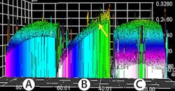
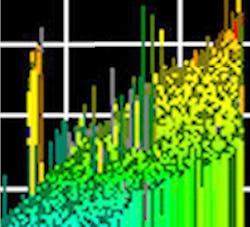
4. Magnified view of the top of raft B, showing spikes caused by voids.
The top portion of raft B in Fig. 3, marked by an arrow, is magnified in Fig. 4. As noted, the spikes that rise above the solder-to-raft interface at the edges of the raft represent modest elevations of the solder between adjacent rafts. But at the center of Fig. 4 are several spikes that are distinctly not near an edge of the raft. These are caused by reflections from the top surfaces of voids that lie between the raft and the solder.
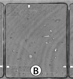
The planar reflection-mode depiction of these voids can also be seen just right of center in Fig. 5, which is a non-3D reflection mode image where the amplitude of a return echo is converted into color or, as here, brightness. Fig. 5 covers a depth from about halfway into the solder to the surface of the raft and a bit beyond. The voids are also visible, although less distinctly, to the right of center in Fig. 1.
5. Planar reflection mode view of raft B. Note the group of voids at right.
In general, if an IGBT module can be imaged acoustically in the reflection mode, it can be imaged in 3D as well. The echoes are the same in both modes, but in reflection mode they’re converted into color, and in 3D into a one-pixel vertical feature. The value of 3D acoustic imaging lies in its handling of significant features. Other modes can measure these features and create planar images, but acoustic 3D makes it easier to visualize their structure.
C-SAM® is a registered trademark of Nordson-Sonoscan.
Tom Adams is a Consultant for Nordson-Sonoscan Inc.
