Members can download this article in PDF format.
What you'll learn:
- Detailed look at the Energy Exchanger architecture.
- The key role played by the fast voltage regulators.
- Evaluation of two different Energy Exchanger architectures: single-ended and fully differential.
As load currents continue to increase in server, and especially AI, applications, while rail voltages tend to decrease, the conduction losses on the PCB become more harmful. The concept of stacked power elements and processing of the power difference are considered possible solutions to this problem.1-4
Specifically, with the Energy Exchanger concept,1 only the power difference is processed. In this architecture, the average current is observed in the system rail, not the minimum current of the elements connected in series.
As losses are generally proportional to the processed power, lowering the processed power generally leads to the loss reduction. Notice that different converters can be used in the Energy Exchanger architecture, including different capacitor circuits.1
Extending this concept to the applications that need aggressive transient management, voltage regulators (VRs) are added to deal with the fast transient loads.2,3 Regarding the low-voltage, high-current applications that target the AI market, a prototype board was built.4 The single-ended Energy Exchanger was implemented with switched capacitor circuits, similar to previously proposed in Reference 3.
As expected, the single-ended Energy Exchanger showed significant noise pollution of the load Vo rails when processing significant power difference. Reported measured system efficiency was ~86% at full load of 250 W, with predicted ~2% improvement if the bias circuits are improved.
Stacked Load System
This work presents a stacked load prototype that achieves >95% efficiency at a full load of 450 W. The critical improvement in the Energy Exchanger also is discussed.
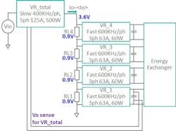
The block diagram of the Stacked Load prototype is shown in Figure 1. The main voltage regulator VR_total delivers full power to the stacked loads with the main objective to be as efficient as possible.
The four fast voltage regulators are responsible for the precise voltage regulation and transient response on each corresponding load rail. If loads are ideally matched, these fast VRs process zero power, and only if there’s a load mismatch, they process power difference.
The fast VRs are thermally designed for much smaller current than the VR_total, as the maximum load difference is assumed to be smaller than the full load. However, it’s important to design fast VRs to be capable of the full-scale transient of each load, because even if all loads are closely matched on average, it’s hard to expect perfectly matched transient steps on all of them. Moreover, it takes longer time for the slower VR_total to adjust the output current.
The Energy Exchanger ensures power exchange among all of the input rails for fast voltage regulation. If VR_total is driving only linear loads connected in series, the output current is determined by the lowest load current. But when the Energy Exchanger is added, the VR_total output current ideally becomes averaged current between all loads. In practice, that current is slightly higher as it compensates for the losses in the fast VRs and Energy Exchanger.
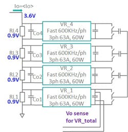
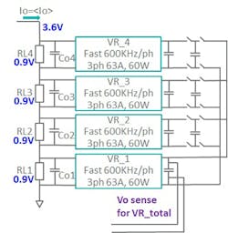
Two different designs for the Energy Exchanger were evaluated: the originally considered single-ended Energy Exchanger shown in Figure 2 and the fully differential Energy Exchanger from Reference 1 shown in Figure 3.
The single-ended Energy Exchanger from Figure 2 has a problem—return currents from each flying capacitor must go through the Co bulk capacitors of the loads in series. These charge-discharge currents have a much faster ac content compared to the output currents of the buck converters (both VR_total and fast VRs).
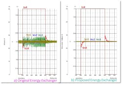
Figure 4a shows the simulated system performance with the single-ended Exchanger, when the load RL4 in Figure 1 has a current step of 50 A. There’s a visible noise on all rails in general, which significantly increases when the Energy Exchanger starts moving charge to the input of VR_4.
This noise problem appears to be fixed in Figure 4b, as the differential Energy Exchanger doesn’t force any currents through the loads or Co bypass of the load rails.
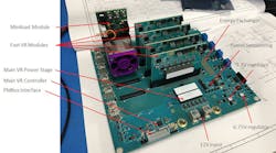
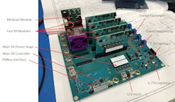
The implemented prototype for the stacked load system is shown in Figure 5. Two versions were designed with only difference in the Energy Exchanger—one design with the single-ended solution from Figure 2, and the second with the differential Exchanger from Figure 3.
Fast transient loads were used to evaluate the dynamic performance, implemented by pluggable modules (only one plugged module for fast transient is shown in the picture). The main board also has connectors for the fast VRs. This arrangement allows for easy adjustment and changes to the fast VR modules.
Measured Results
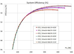
Figure 6 shows the efficiency of the complete system operating with balanced load, including all of the bias circuitry from 12-V input and control. Load voltages were tested at 0.8, 0.9, and 1.0 V.
The efficiency performance is very close between the two different Energy Exchanger options, EE1 and EE2, and in the nominal operating conditions, Vo = 4 × 0.9 V = 3.6 V reaches more than 95% at full load. Notice that placing all loads in parallel corresponds to 500-A current into a single Vo = 0.9-V rail.
Achieved >95% system efficiency noticeably outperforms published efficiency data for these conditions. High efficiency is driven by two main factors: 4X output current reduction as four loads are connected in series, and that the main VR_total delivers full power into 4X higher Vstack voltage (4 × Vo), as higher Vo generally improves VR efficiency.
While this is a prototype board with off-the-shelf parts and no optimization of components, the achieved high efficiency is in part credited to coupled inductors used in the main VR_total, as well as fast VR modules.
Generally, coupled inductors are allowed to keep switching frequencies low in a given reasonable size, keeping the switching loss down. This is especially important for the fast VRs, because in the case of balanced load, these VRs don’t process much power, but still have switching losses that ideally need to be decreased.
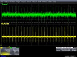
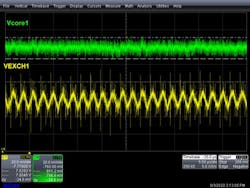
The big difference in the operation of the two different Energy Exchangers is illustrated in Figures 7 and 8, showing voltage ripple on the first Vo1 rail and VR1 input supply rail. The conditions for both are the same: the Vo4 rail is loaded by Io = 50 A; all other rails are at zero current. Therefore, the Energy Exchanger is moving a lot of power from the other rails to supply the rail Vo4.
The single-ended Energy Exchanger drives large spikes through the parasitics of Co on the Vo1 rail (also clearly a problem in the case of Reference 4), while the differential Energy Exchanger just leaves the Vo rail intact, with only a small ripple at much slower time scale that relates to the buck-converter currents (not the switched-capacitor circuits).
The most important impact is the reduction of the fast voltage spikes from >60 mV (>6.6% of Vo = 0.9 V) in case of the single-ended Energy Exchanger to <25 mV (<2.8% of Vo = 0.9V) in the case of the differential one. In the latter case, the voltage ripple has no high-frequency spikes at all, only a ripple associated with the ripple current in the buck converters. The result matches the expected trend from the simulations.
The fast spikes on the supply rail are potentially harmful to the digital circuitry and it’s important to mitigate the issue. As Vo values are expected to decrease further, the same amplitude of the noise has a larger impact on the operation of the fast loads.
Noise improvement also is implemented with the differential Energy Exchanger in Figure 3 by phase shifting among switching events for the different flying capacitors. Notice that it’s not possible for the single-ended circuit in Figure 2; all capacitors must be switched at the same times.
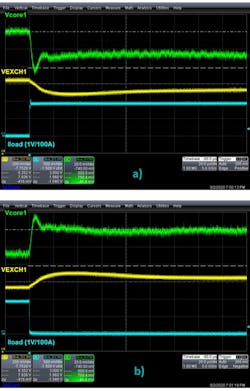
Fast transient performance is shown in Figure 9: loading (a) and unloading (b) 100-A steps on rail Vo1. The other rails are unloaded. So, while initially the fast VR1 delivers all 100 A, the averaged 25 A comes from the VR_total and the fast VR1 supplies only 75 A to the 100-A load.
Looking at the changing droop on the Vo1 rail, notice that it takes approximately 10 µs for the VR_total to deliver 25-A average current, which decreases the fast VR1 droop proportionally. Correspondingly, VR2, VR3, and VR4 subtract 25 A from their rails and move that power into the Energy Exchanger and VR1. The Energy Exchanger voltages are unregulated. As a result, it takes longer than 10 µs to settle the input rail for the fast VR1 (yellow trace).
Conclusion
The fully functional stacked load prototype was implemented and showed efficiency generally higher than in traditional architectures for the same Vo and total Po (>95% at Vo = 0.9 V at Po = 450 W). The prototype board was made with off-the-shelf components; the actual optimization for customer specifications potentially lead to even higher performance.
The concept of stacked load power delivery shows good promise in improving efficiency, with a dramatic decrease in distribution losses and the main VR operating at higher efficiency due to increased load voltage Vstack.
Notice also that the significant decrease of load current should bring more improvements in PCB losses when the loads are densely packed. In other words, actual customer application with very dense high current and low-voltage load creates a bigger challenge for the distribution losses. Thus, the improvement due to stacked load architecture is higher than on some prototype boards.
Building on the earlier developed Energy Exchanger concepts,1 the differential Energy Exchanger for floating rails showed much better noise behavior for the load voltage rails. Any fast current and related voltage spikes were eliminated in any loading conditions.
References
1. A. Ikriannikov and A. Stratakos, “System, method, module, and energy exchanger for optimizing output of series-connected photovoltaic and electrochemical devices.” U.S. Patent 9,331,499, filed April 2011.
2. E. Candan, P. Shenoy, and R. Pilawa-Podgurski, “A Series Stacked Power Delivery Architecture with Isolated Differential Power Conversion for Data Centers.” IEEE Transactions on Power Electronics, vol. 31, No. 5, May 2016.
3. S. Jiang; G. Sizikov; M. Popovich, “Power balancer for series-connected load zones of an integrated circuit.” U.S. Patent 10,985,652, filed March 2020.
4. K. Kshirsagar, D. Clavette, P. Kasturi, and W. Huang, “Power Loss Reduction in Power Distribution Network Through Vertical Stacking.” Industry Session in IEEE 2021 Applied Power Electronics Conference, June 2021.
