What you'll learn:
- The impact of materials on designing reliable devices.
- How packaging plays an important role in SiC MOSFET design.
- Determining the FIT rate for SiC MOSFETs.
There’s no doubt that the material properties of wide-bandgap materials like silicon carbide (SiC) allow for higher performance than silicon-based (Si) structures. But matching or even exceeding the reliability of Si devices requires innovations in design and rigorous test and evaluation to meet customer requirements.
SiC’s advantage in power switching designs is in large part a function of the material properties. The 10X higher dielectric breakdown strength compared to silicon enables fast unipolar high-voltage devices with low area-specific on-resistance (RDSon). That advantage allows for higher power density and/or simplified cooling approaches for designing power supplies or other switching systems.
Design of consistently reliable devices, however, must take into account differences in the physical properties of power semiconductors based on the different materials. In particular, the defect footprint at the interface of SiC and its substrate material, SiO2, leads to low-channel mobility. To compensate for this deficiency, the applied electric field at on-state, especially in planar SiC MOSFETs, is greater than with Si MOSFETs (4 to 5 MV/cm compared to 3 MV/cm in a silicon device).
The result of the higher field values is oxide field stress in the on-state. Today’s SiC MOS devices have much higher-defect densities at the planar interface than what’s typically seen in Si-based devices.
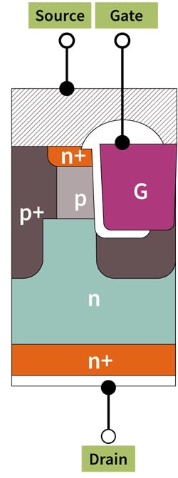
In terms of device geometry, the commonly used planar approach to MOSFET cell design leads to stress at two points of the interface—at on-state between gate and source for the reason mentioned above, and the gate drain overlap in blocking mode. To minimize the stress in on-state, Infineon adopted a trench MOSFET cell structure for its SiC MOSFETs (Fig. 1) whereby the field stress is primarily isolated to the trench corners at reverse bias.
In on-state, no excessive fields are required since the defect density at the 90-deg. tilted crystal face is much lower. In the cell design (Fig. 2), the electric field in the gate oxide is limited in both the on-state and the off-state to achieve the desired on-resistance while meeting requirements for performance and reliability.
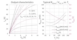
In a trench cell, the electric field in the gate oxide is limited in both the on-state and off-state while meeting specific on-resistance targets. Low on-resistance is achieved with driving voltage (VGS) of 15 V at a typical gate-source-threshold voltage of 4.5 V, which is a benchmark in the landscape of SiC transistors. Figure 3 illustrates output characteristics of an Infineon 1200 -V SiC trench MOSFET at room and high temperature, as well as variability of on-resistance as a function of temperature.
Packaging is the Key to Realizing SiC Benefits
Switching performance in target applications is, of course, the end goal for MOSFET devices. In this respect, a principal characteristic of SiC MOSFETs that impacts switching capability (SC) and switching losses is capacitance. Package design plays an important role in minimizing switching losses, which are mainly turn-on losses. Kelvin contacts are preferred since they separate the current in load and control paths, and therefore help prevent di/dt induced feedback that may increase dynamic losses.
Thermal performance also is an important criterion in package selection. While SiC generally has lower absolute losses, those that do occur are concentrated in small areas of the chip. Low stray inductance helps manage high di/dt slopes and minimize critical voltage peaks.
In addition, particularly for multichip packages of parallel die, designs supporting a symmetric arrangement of chips are needed. For these reasons, a TO-247-4 type package is an ideal solution for a discrete device and a module like the Infineon EASY platform.
Testing Enables Low FIT Rate and High Gate-Oxide Reliability
Given a cell structure that reduces oxide field stress, Infineon examined the reliability and ruggedness of the SiC trench MOSFET with the goal of optimizing the design for best possible field reliability. Ruggedness is the ability of a device to withstand extraordinary stress, such as short-circuits or pulse currents. Reliability deals with device stability in operation over a defined lifetime. This is typically quantified as failure-over-time (FIT) rate, which is a statement of how many failures are acceptable over a period of time.
The two factors involved in reliability are cosmic ray effects and gate-oxide stability, with the effective total FIT rate determined as the sum of the two (Fig. 4). A figure for cosmic ray effects is determined in the same manner as in Si-based devices, with experimentation for the specific technology setting a target level. This is a well-established practice, typically addressed by optimizing electric field distribution in the drift zone of the device.
Low-oxide FIT rates for SiC are achieved by screening as a function of manufacturing QA. The goal of such screening is to reduce the number of devices affected by extrinsic defects to 10 ppm or less. Electrical screening is the typical test methodology in production.
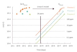
Infineon used accelerated gate-oxide stress tests to assess the on-state reliability of SiC MOSFETs for 100 days at 150°C. Sample groups of 1,000 devices each were subjected to three stress runs at different positive gate-stress biases, with typical results seen in Figure 5. Through optimizations based on test findings, the gate oxide was tuned to reduce failures from less than 10 of 1,000 devices at 30 V (twice the recommended gate bias) to only one fail out of 1,000 and to zero fails at 25 V and 15 V.
Off-state oxide stress, which is controlled by shielding sensitive areas by proper design of p-regions, was also refined through repetitive stress tests and fine-tuning of the cell design. Final production level for device families is determined when stress testing of 5,000 devices for 100 days at 150°C, VGS = −5 V, and VDS = 1000 V results in zero device failures.
Conclusion
Methodical design, test, and fine-tuning of parameters such as gate-oxide thickness described here in relation to 1200-V SiC MOSFETs is mirrored in Infineon’s 650-V CoolSiC MOSFET family. The company’s goal is to provide designers with devices offering unmatched efficiency and reliability for hard- and resonant-switching applications across its range of power-conversion and -supply applications.


