A chess grandmaster, who also happens to be an electronics hobbyist, decides to design his own chess clock. The LEDs, normally open pushbutton switches, and microcontrollers are all in place, driven by a pair of 1.5-V AA batteries. However, the clocks only last for a few hours. So he checks online for a power-management IC to extend the battery life, and finds one promising 94% efficiency. After purchasing the chip and ramming it onto a prototype, he becomes puzzled when the operating lifespan changes only slightly. He then re-checks the wires and solders and connections in a vain effort to find a solution.
Let’s take such a scenario to the industry level. Apple is designing its 23rd Iphone. The company producing the processor for the Iphone23 is looking for a PMIC that can deliver a transient response of around 10 mV with a 10-A shifting load (absurd!). They contract a semiconductor company to design the chip. After numerous tedious design reviews, the PMIC becomes ready. Trouble ensues, though, when the chips are tested in tandem with the processor. The chip is oscillating at 8 A! And the processor is toggling between an on and off state. What happened here?
Certain measurement plots and point data in IC datasheets can mislead consumers into believing that the IC possesses a certain set of electrical characteristics that aren’t exactly 100% true, due to the limitations and imperfections of the measurement procedures done in yielding those plots and data. In this article, I elaborate on those limitations and imperfections, and hope to give readers a deeper insight on the matter.
Regarding the latter example, such dilemmas occur less frequently due to the presence of field application engineers (FAEs). They are there to specialize in the evaluation of the product, and if a problem occurs such as an oscillating output at 8 A, they can analyze and debug on the problem.
However, in the absence of FAEs, the designer faces the problem alone. With the problem being handled from a singular perspective, the underlying cause (usually a misunderstanding of the consumer’s required specifications) has a smaller probability of being properly addressed.
To aid in the explanation of the points in question, let’s do an analysis of the datasheets of a PMIC for processors of mobile applications, a motor driver, and a low-power dual operational amplifier.
MC34708 Power-Management IC for i.MX50/53 Families (Freescale Semiconductor)
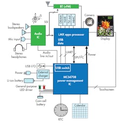
The MC34708 is a power-management IC (PMIC) designed for use with the Freescale i.MX50 and i.MX53 families (Fig. 1). Typical applications include tablets, smart mobile devices, and portable navigation devices. It’s lead-free and available in two package sizes (do you still happen to stumble upon any commercial ICs that don’t label their products lead-free?). It offers six bucks, a boost, eight LDOs, USB/UART/audio switching for a mini-micro USB connector, a 10-bit Coulomb counter, an RTC, and of course, an SPI/I2C interface for external control. The device doesn’t support battery-charger management, though.
Looking at the block diagram, we get a view of how the entire system is supposed to function. I’m not going to quote all of this PMIC’s features (a 159-page document is available for public download… ugh) except for some plots and data.
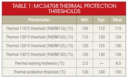
Let’s start with the thermal characteristics. Table 1 shows a representation of the datasheet’s thermal protection thresholds for MC34708. It says to set ADEN to 1 to enable thermal monitoring. Signals will be generated to identify whether the chip has exceeded 110, 120, 125, or 130°C. Upon crossing the 140°C threshold, the chip will shut down.
Now, anyone who has any experience with testing a chip’s thermal characteristics will tell you that doing so is not quite straightforward (this explains the minimum and maximum margins). First, what kind of thermocouple is being used? Most semiconductor companies would use a type T thermocouple, because the testing range usually falls in between –175 to 225°C. In fact, typical thermo streamers can only give around –70 to 200°C (at 300°C, the heater can damage itself after prolonged exposure). Type T thermocouples have a tolerance of ±1°C, which already reveals a lot about the accuracy of the reading.
Another factor to consider is the soak time (the amount of time that elapsed after the chip is exposed to the set temperature). In spite of the thermocouple indicating that the set temperature was reached, I’ve experienced getting two different measurement readings at two different intervals after soaking a device under test (DUT), especially when it is a low voltage/low current measurement. Of course, the latter reading would be the more appropriate measurement, since higher soakage times mean that it’s more probable the system achieved steady-state.
Another point of intricacy concerns the physical setup. If the chip is at 125°C, are the adjacent external components, such as inductors, capacitors, and resistors, also at that temperature? Is the thermocouple also placed directly above the DUT or a little bit above it? Did the evaluator use a thermostreamer or a hot air rework station? Or perhaps a soldering iron (in the extreme case)?
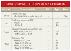
Now let’s move on to the electrical specification. Table 2 is a representation of some electrical specifications of SW1, one of the buck regulators, in the datasheet.
The turn-on time is pretty clear, from 50% of the enable signal to 90% of the end value. The switching frequency can be either 2 MHz or 4 MHz by toggling PLLX. The quiescent-current consumption is at 240 µA at APS mode and 15 µA at PFM mode. This is a low-current measurement, and is prone to errors by environmental factors and instrument setting (remember to set the ammeter to the lowest range). Note that at PFM mode, the quiescent current is significantly lower with a 0-mA load (because PFM is best used with low loads).
The presentation of efficiency in this datasheet is unique, since it does so in tabular form. Usually, efficiency is expressed in curves. Given the point data, we don’t know whether the efficiency would dip between a 1- and 200-mA load (it’s pretty unlikely if you’ve seen other efficiency curves). Also, efficiency is more sensitive than quiescent-current consumption because the measurement depends on both the very low off current of SW1 and the actual input voltage, output voltage, output current, and ambient temperature (yes, just a slight change in TA can ruin the entire efficiency measurement, requiring re-measurement of the off current).
L293 Quadruple Half-H Drivers (Texas Instruments)
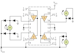
The L293 is designed to drive inductive loads as well as other high-current and high-voltage loads (Fig. 2). It features a wide supply-voltage range and separate input logic supply. It also includes internal ESD and TSD protection. The device drives a typical output current of 1 A per channel up to a maximum of 2 A. Output clamp diodes for inductive transient suppression are visible in the block diagram.
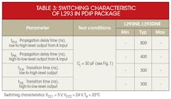
Now let’s focus on the switching characteristics. Table 3 shows the typical delay and transition times of the L293 in a PDIP package.
One time there was a design engineer from XY company who received a customer complaint over a motor driver product. “Darn it, what IC did you give me? This isn’t the propagation delay time I asked for!” exclaimed the indignant costumer. The design engineer humbly countered. “But isn’t this value that we agreed upon?” The customer replied “Yes, it is. But that is not what I’m getting here on my end. In fact, I’m getting a much shorter delay time!”
After a few bouts, both parties discovered that they had different definitions of the delay time. The designer understood it as a point from 50% to 90% or 10%, while the customer understood it as 50% to 50%. Consequently, the design engineer constructed a circuit with a propagation delay much longer than what the customer envisioned.
Looking at the L293, one good question to ask is what reference levels were used to define those 800-ns and 400-ns low-to-high and high-to-low propagation delay times. Closer inspection of the datasheet would show that the propagation delay was measured from 50% to 50%. This is useful information that shouldn’t be ignored, and it could save the consumer from the pitfall described above.
LMx58-N Low-Power, Dual Op Amps
The LMx58 consists of two operational amplifiers. It is internally frequency-compensated for unity gain with a large dc voltage gain of 100 dB and 1-MHz bandwidth. It features a low input offset voltage of 2 mV and its input bias current is temperature-compensated. I think the block diagram is straightforward (two op amps), so it’s not included here.
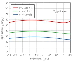
The plot above (Fig. 3) shows a temperature sweep while simultaneously measuring the input current. It isn’t feasible to sweep the temperature over all voltages, so if a problem occurs, say at hot temperatures and at a voltage of 10 V, the troubleshooter shouldn’t exclude the possibility of the input current going awry. That’s because the characteristic isn’t actually evaluated at that condition.
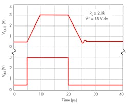
Looking at Fig. 4, there’s no definition of the rise and fall times used for the input voltage pulse. If the consumer were to use different rise or fall times, there’s a chance that the output pulse would have a different rise and fall time other than the observed 5 µs. On the other hand, I don’t know the sensitivity of the circuit to a varying rise and fall time, so it could be negligible.
Conclusion
Identifying the limitations of a datasheet saves lots of time in terms of troubleshooting and redesigning circuits. It also proves economical, since it helps to avoid expenses incurred with re-manufacturing a product. At the same time, an in-depth analysis of the datasheet gives those assigned in product support a better chance to identify the source of the conflict, as well as equip them with a firm understanding of the product’s behavior.

