What you’ll learn:
- A Linux-based open-source development platform for EV charging stations promises to accelerate development and enhance interoperability.
- Advanced packaging is playing an increasingly important role in enabling more compact, cooler-running designs in a wide range of consumer and commercial applications.
- Solid-state circuit breakers and other protection devices are beginning to displace the century-old electromechanical solutions that have dominated the market until now.
Developing reliable, interoperable EV chargers that support the latest communications protocols between electric vehicles (EVs) and charging stations has become easier and faster, thanks to a joint project between the Joint Office of Energy and Transportation (Joint Office) and the Linux Foundation (LF).
The project, which began in January 2024, was formed to build open-source software tools to support communications between EV charging infrastructure and other systems through LF Energy’s EVerest project. The Joint Office announced that the March release of EVerest includes support for the communication protocol requirements defined in the National Electric Vehicle Infrastructure Standards and Requirements . It enables Plug and Charge functionality so that drivers can simply connect their vehicle to a charger to authenticate, charge, and pay.
Joint Office open-source software experts are now working with the EVerest community to advance production-ready deployments of the software by early adopters like Enteligent, Jule, and Voltpost. These EV charging ecosystem players are using EVerest to advance a variety of pioneering projects, including:
- Enteligent Inc. develops DC-coupled electric-vehicle service equipment (EVSE) and solar-power optimization technologies. The company’s first EVSE product, the TLC-EV charger, uses EVerest in its full-stack environment for charging management.
- Jule is currently working on its ISO 15118 implementation leveraging the EVerest framework. The team has been able to integrate the code base into its hardware development kit. They achieved both a board implementation of control pilot and supported state machine, and established an initial charger to vehicle SLAC communication.
- Voltpost is developing Level 2 chargers that retrofit lampposts to deploy chargers more easily to densely populated urban areas. Voltpost has been working with the EVerest community over the past several months to understand how to deploy it to production.
EVerest provides a focal point for the electric mobility community to collaborate on the development of fundamental communication protocols. EVerest also accelerates the release of new features, modifications, and charger customizations faster than other software options, offering a reliable and future-proof charging solution.
The EVerest reference implementation is available on GitHub for EV charging industry players to leverage for compliance and interoperability. In addition, single-line demos showcasing the functionality of the implementation are available.
An article with full details on this development can be found here.
STMicroelectronics has commenced production of automotive high-side power switches that feature proprietary intelligent fuse protection and a serial peripheral interface (SPI) for diagnostic data, permitting enhanced resilience and functional safety.
The quad-channel VNF9Q20F is the first in a new family of monolithically integrated devices that combine ST’s advanced VIPower M0-9 MOSFET and proprietary STi2Fuse technology. Based on patented I2t (current squared through time-to-fuse) functionality, the STi2Fuse responds within 100 µs to turn off the MOSFET if excessive current is detected.
Performing as an intelligent circuit breaker, the VNF9Q20F enhances overall board voltage stability and prevents PCB traces, connectors, and wire harnesses from overheating. In addition to preventing damaging overloads, ST’s new automotive power switch also has a capacitive charging mode that enables harmless inrush currents, thereby permitting normal operation with highly capacitive loads.
Equipped with the functionality to support the latest zonal electrical/electronic architectures, the VNF9Q20F can also be used for fuse and relay replacement, ECU isolation, and managing systems that are active when the vehicle is parked. With 64 programmable current-limit values, the STi2Fuse lets designers determine the overload response with high precision.
The intelligent high-side switch integrates several advanced internal features, including a 10-bit analog-to-digital converter (ADC) and fault registers that support rich diagnostic information and digital current-sense feedback. These functions can be used to support advanced vehicle capabilities such as predictive maintenance.
By providing diagnostics through the SPI, and with built-in self-test, the VNF9Q20F enables systems to meet specified safety integrity levels in accordance with ISO 26262. An embedded failsafe mode preserves operational status in the event of a failure or malfunction.
Housed in a 6- × 6-mm QFN package, the VNF9Q20F costs from $2.850 for 1,000 pieces.
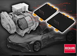
Four new models were added to ROHM Semiconductor’s TRCDRIVE pack series of molded silicon-carbide (SiC) modules. These 2-in-1 integrated SiC devices include two 750-V-rated (BSTxxxD08P4A1x4) and two 1,200-V-rated (BSTxxxD12P4A1x1) that are optimized for use in electric-vehicle traction inverters.
They’re housed in a compact TRCDRIVE pack that supports up to 300 kW and features a unique terminal configuration. This helps solve some of the challenges involved with traction inverters in terms of miniaturization, higher efficiency, and reduced assembly costs.
SiC devices promise to enable the development of electric powertrain systems that are more efficient, compact, and lightweight. However, achieving low loss in a small size has been a difficult challenge.
To solve these challenges, ROHM developed SiC molded-type modules specifically for traction-inverter drive applications based on a unique structure that maximizes heat dissipation area. They incorporate the company’s 4th generation SiC MOSFETs with low on-resistance to yield an industry-leading power density (roughly 1.5X higher than typical SiC molded modules).
The modules are also equipped with control signal terminals using press-fit pins, enabling easy connection by simply pushing the gate-driver board from the top, considerably reducing installation time. In addition, low inductance (5.7 nH) is achieved by maximizing the current path and utilizing a two-layer busbar structure for the main wiring, contributing to lower losses during switching.
To make these products widely available and cost-effective, ROHM established a high-volume production system that can yield up to a 30X increase in production capacity, as compared to conventional SiC case-type modules.
The TRCDRIVE pack is scheduled to be launched by March 2025 with a lineup of 12 models in different package sizes (small/large) and mounting patterns (TIM: heat dissipation sheet/Ag sinter). In addition, ROHM is developing a 6-in-1 product with built-in heatsink.
Power Integrations enhanced its hardware-software bundle for brushless DC (BLDC) motors with BridgeSwitch-2, a new high-voltage integrated half-bridge (IHB) motor-driver IC family targeting applications up to 1 HP (746 W). The new ICs, which feature high- and low-side drivers and advanced FREDFETs with integrated lossless current sensing, deliver inverter efficiency of up to 99%.
IHB architecture eliminates hot spots, which increases design flexibility and reliability, slashes component count, and saves PCB area. BridgeSwitch-2 is supported by Power Integrations’ MotorXpert software suite that includes single-phase trapezoidal control and three-phase, sensorless field-oriented-control (FOC) modules, speeding inverter development.
BridgeSwitch-2 ICs handle operational exceptions in hardware, which permits the use of IEC 60730 Class A safety software, shrinking certification time by months. Quiescent BLDC inverters can be ordered into sleep-mode, reducing driver power consumption to less than 10 mW. This leaves more power available under regulated standby power limits to be allocated for loads such as network access and monitoring.
The ICs address a power range of 30 to 746 W (1 HP), encompassing applications ranging from heat exchanger fans, refrigerator compressors, fluid and circulation pumps, and gas boiler combustion fans to washing machine drums and kitchen blenders and mixers. The IHB architecture reduces component count by 50% and PCB space by 30% over discrete designs by eliminating shunt resistors and associated signal conditioning circuits. Shunt losses are also eliminated, improving efficiency.
Precise motor control is achieved with the built-in real-time reporting of phase-current (IPH) information. Accurate turn-on/off gate drive and a soft-body diode result in a typical EMI profile 10 dB lower than existing drivers, enabling a smaller EMI filter to be selected.
BridgeSwitch-2 ICs feature built-in DC overvoltage protection and current limits that protect the inverter and the system without relying on system software. The choice of error-flag or comprehensive fault bus reporting supports a range of system requirements.
Emerging use cases like failure prediction are now possible with the high accuracy of the built-in IPH information and comprehensive reporting via the fault bus. BridgeSwitch-2 motor drives use built-in, hardware-based, low- and high-side overcurrent protection to meet IEC 60335-1 Class A requirements. BridgeSwitch-2 also works without an auxiliary power supply, further reducing PCB area and component count.
Pricing for BridgeSwitch-2 ICs starts at $0.48 for 10,000-unit quantities. A 15- W reference design and design report, RDK-974, can be freely downloaded.
Cambridge GaN Devices (CGD) launched its lowest-ever on-resistance (RDS(on)) parts that have been engineered with a new die and new packages to deliver the benefits of gallium nitride (GaN) to high-power applications such as data centers, inverters, motor drives, and other industrial power supplies. New ICeGaN P2 series ICs feature RDS(on) levels down to 25 mΩ, supporting multi-kilowatt power levels with the highest efficiency.
Incorporating an on-chip Miller clamp to eliminate shoot-through losses during fast switching and implementing 0-V turn-off to minimize reverse conduction losses, ICeGaN ICs outperform discrete e-mode GaN and other incumbent technologies.
The new packages offer improved thermal-resistance performance as low as 0.28 K/W. The dual-gate pinout of the dual-side DHDFN-9-1 (dual heat-spreader DFN) package helps optimize PCB layout and simplify paralleling for scalability, enabling customers to address multi-kilowatt applications with ease. The new packages were also engineered to improve productivity, with wettable flanks to simplify optical inspection.
The P2 Series ICeGaN power ICs are sampling now. The family includes four devices with RDS(on) levels of 25 and 55 mΩ, rated at 60 and 27 A, in 10- × 10-mm footprint DHDFN-9-1 and BHDFN-9-1 (bottom heat-spreader DFN) packages. In common with all CGD ICeGaN products, the P2 series can be driven using any standard MOSFET or IGBT driver.
Two demo boards feature the new P2 devices: a single leg of a three-phase automotive inverter demo board, developed in partnership with the French public R&I institute IFP Energies Nouvelles; and a 3-kW totem-pole power-factor-correction demo board.
According to Qorvo, it’s rolled out the industry's first 4-mΩ SiC junction field-effect transistor (JFET) in a TOLL package. It was designed for circuit protection applications, including solid-state circuit breakers, where low resistance, superior thermal performance, small size, and reliability are paramount.
With its RDS(on) of 4 mΩ, the UJ4N075004L8S offers the lowest on-resistance among the 650- to 750-V class of power devices in standard discrete packages. This low RDS(on) significantly reduces heat generation and, when coupled with a compact TOLL package, enables a solution size that is 40% smaller than competing devices in TO-263 packages.
The compact solution enables designers to work easily within the space-limited dimensions of today’s electromechanical circuit breakers. Meanwhile, its low losses allows it to operate without the need for elaborate cooling systems.
Qorvo’s robust JFETs are well-suited to meet the challenges of circuit protection, providing the ability to turn off at very high inrush currents during circuit faults. The latest JFET can also withstand high instantaneous junction temperatures without experiencing degradation or parametric drift. The normally-on nature of the device lends itself to seamless integration into systems where the switch is in the on-state by default and in turn-off state under fault conditions.
The UJ4N075004L8S is now available for sampling and will enter full production in Q4 2024, accompanied by additional JFET options, including 750 V with 5-mΩ ratings and 1,200 V with 8-mΩ ratings, all in TO-247 packaging. For more details, visit Qorvo’s Power Solutions site.
An advanced 650-V, 10-A SiC Schottky diode developed by Nexperia is now automotive qualified (PSC1065H-Q) and available in real-two-pin (R2P) DPAK (TO-252-2) packaging. In addition, the company now offers industrial-grade devices with current ratings of 6, 16, and 20 A in TO-220-2, TO-247-2, and D2PAK-2 packaging to facilitate greater design flexibility.
These diodes address the challenges of demanding high-voltage and high-current applications, ranging from switched-mode power supplies, AC-DC and DC-DC converters, and battery-charging infrastructure to motor drives, uninterruptible power supplies, and photovoltaic inverters for sustainable energy production.
The merged PiN Schottky (MPS) structure of these devices provides additional advantages over similar competing SiC diodes, including enhanced robustness against surge currents. This eliminates the need for additional protection circuitry, thereby significantly reducing system complexity and enabling hardware designers to achieve higher efficiency with smaller form factors in rugged high-power applications.
In addition, Nexperia’s “thin SiC” technology delivers a thinner substrate (one-third of its original thickness), which dramatically reduces the thermal resistance from the junction to the back-side metal. This results in lower operating temperature, higher reliability and device lifetime, higher surge-current capability, and lower forward voltage drop.
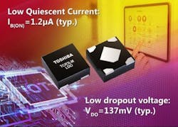
A new series of low-dropout (LDO) voltage regulators developed by Toshiba Electronics comes in the company’s ultra-miniature DFN4D package type. Specifically aimed at miniature applications powered by small-scale batteries, the new family of devices significantly reduces power consumption, thereby elongating the usable lifetime.
The new TCR3LM series offers a comprehensive lineup of over 30 devices spanning 0.8 to 5.0 V DC with an input voltage (VIN) of 1.4 to 5.5 V DC. Each device is capable of delivering up to 300 mA of output current (IOUT).
Enhanced drop-out performance features a typical dropout voltage (VDO) of just 137 mV. Output voltage can be achieved with a lower input voltage, so battery drain is reduced. Furthermore, improved load transient response boosts the output stability when the load fluctuates. Typical transient response is −70 mV/+35 mV at 2.8-V output, and quiescent current (IB(ON)) is reduced to a typical value of 1.2 μA.
The ultra-compact solution comes in a DFN4D package measuring 1.0 × 1.0 × 0.37 mm. Furthermore, small ceramic capacitors can be used on the input and output, shrinking the overall solution size even further. Despite its small size, these feature-rich LDO regulators offer overcurrent and overtemperature protection as well as an auto-discharge function.
The new TCR3LM series, comprising the TCR3LM08A, TCR3LM18A, and TCR3LM33A, is now in mass production.
Alpha and Omega Semiconductor Limited recently introduced its AONG36322 XSPairFET designed for space-constrained DC-DC applications. The new device features two 30-V MOSFETs in a half-bridge configuration, where the high- and low-side MOSFETs are in an asymmetric DFN3.5x5 XSPairFET package.
With this innovative design, the AONG36322 can replace an existing DFN5x6 asymmetric half-bridge MOSFET with an approximate 60% space-saving solution. The AONG36322 is intended to open the door to a new generation of more compact applications such as point-of-load (POL) computing, USB hubs, and power banks.
The AONG36322 is an extension to the AOS XSPairFET lineup, designed with the latest bottom-source packaging technology. Its integrated high- and low-side MOSFETs feature 4.5 mΩ and 1.3 mΩ maximum on-resistance, respectively, where the low-side MOSFET source is connected directly to the exposed pad on the PCB to enhance thermal dissipation. The AONG36322 package design also delivers lower parasitic inductance, significantly reducing switch node ringing.
The AONG36322 is immediately available in production quantities, with a lead time of 16 weeks. The unit price in 1,000-piece quantities is $0.915.


