What you'll learn:
- Features of the ADA4510-2 dual-channel 40-V op amp.
- Features of the LT9890 150-V current monitor.
- Layout recommendations and packaging of the LT9890.
Even as IC functionality, complexity, and level of integration continues to grow, the analog-centric IC vendor community still retains its ability to devise and develop single-function, tightly focused devices. These components generally do only one or a few things. However, they do so crisply, using unique twists so that they can act as nearly complete solutions to the user’s problems.
This scenario is clearly seen in a pair of very different ICs from Analog Devices, with one for precision analog front ends and the other for power management.
ADA4510-2: The Precision Dual-Channel 40-V Op Amp
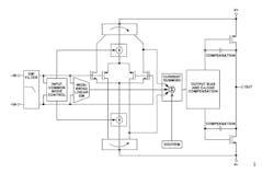
For precision analog-signal amplification, the ADA4510-2 is a dual-channel, 40-V precision, CMOS rail-to-rail input/output op amp, delivering excellent DC precision and high AC performance (Fig. 1). Thus, it’s an appropriate choice for a wide variety of sensor-driven signal-chain applications.
The robust multiplexer-compatible architecture enables the ADA4510-2 to effectively solve common system-distortion and settling problems while providing the very high accuracy required in precision signal chains and front ends. Its specifications feature many desirable low and high values. In the “low” category of attributes, it offers:
- Low offset voltage drift: ±0.07 μV/°C (typical)
- Low offset voltage: ±5 μV typical, ±20 μV (maximum)
- Low voltage noise: 1 μV p-p from 0.1 Hz to 10 Hz (typical)
- Low voltage-noise density: 5 nV/√Hz (typical) at f = 1 kHz
- Low input bias current: ±10 pA (maximum)
- Low THD: −134 dB at f = 1 kHz
- Low quiescent supply current: 1.45 mA per amplifier (typical)
For the “high” category, it features:
- Wide gain bandwidth product: 10.4 MHz (typical)
- High slew rate: 19 V/μs (typical)
- High common-mode rejection: 140 dB (typical)
This amplifier uses Analog Devices’ proprietary DigiTrim technique to achieve a higher degree of precision compared to previous CMOS amplifiers. This technique is a method of trimming the offset voltage and the offset-voltage temperature drift of an amplifier after assembly. It corrects any offset voltages and drifts caused by mechanical stresses during assembly, as well as simplifies temperature calibrations in precision designs.
Integration of EMI Filters
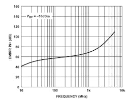
Many of the applications for this device involve low-level signals in the presence of EMI. Op amps in general don’t amplify EMI or RF signals due to their relatively low bandwidth. However, due to the nonlinearities of the input devices, op amps can rectify these out-of-band signals, which then appear as a DC offset at the output. The ADA4510-2 is designed with integrated EMI filters at the input stage of the op amp and includes a graph showing its EMI rejection ratio (EMIRR) (Fig. 2).
The 29-page datasheet includes the expected min/max/typical tables along with nearly 100 performance graphs and application circuits with analysis. Many of the graphs are histograms that show the expected “spread” of results for key performance parameters. The ADA4510-2 is specified from −40 to +85°C and −40 to +125°C, operating from 6 to 40 V or ±3 to ±20 V. Available in a standard 8-lead small outline IC (SOIC) package, it’s priced at $2.59 (500 units).
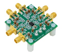
In addition to the datasheet, there’s further support via the EVAL-ADA4510-2 evaluation board (Fig. 3) with edge-mounted SMA connectors for quick prototyping.
The evaluation board, with its own seven-page UG-2133 User Guide, has provisions for photodiode sensors to support easy configuration of a transimpedance amplifier (TIA). The layout is optimized with provisions for guarding to ensure low leakage and low parasitic capacitance for TIA applications.
LT9890: The 150-A Current Monitor for Processor Systems
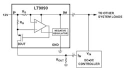
For high-current processor-related current monitoring, the LT9890 150-A current monitor for Intel Psys (Platform Power) and other processor-system applications provides high-precision performance with its internal current-sense element—no discrete external sense resistor is needed. It achieves minimal power loss thanks to its integral, 150-μΩ current-path resistance and an aspect ratio that’s conducive to wide printed circuit board (PCB) traces. Its internal block diagram and use in a typical application circuit is the epitome of simplicity (Fig. 4).
Applications include computers and network servers, Intel central processing unit (CPU) motherboards, network storage systems, communication equipment, electric vehicles, and photovoltaics. The LT9890 is compatible with the Intel Psys Platform Power applications, which enhances processor power management. (With the Psys system, the system designer can use the processor power-control settings to manage and match the platform power-delivery and thermal solution.)
The 26,600:1 input-to-output current ratio (5 mA at 133 A), along with a response bandwidth greater than 3 MHz, provides a fast and accurate ground-referenced output signal while being insensitive to ground-voltage variations. The factory calibration of the current-sense element and a zero temperature-coefficient architecture results in less than 1.3% total unadjusted error (TUE).
When it comes to sense resistors and losses, the value of the sense resistors is a classic design tradeoff between IR voltage drop and I2R power dissipation, versus obtaining and sensing a larger voltage with better SNR. With the LT9890, minimal power loss results from both the low, 150-μΩ current-path resistance as well as a physical aspect ratio that’s conducive to wide PCB traces.
Optimizing Layout When Using the LT9890
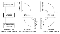
To guide the circuit layout, the datasheet shows three possible routing methods for copper through the LT9890 (Fig. 5). The left-most method is best because it places the device directly in the path from the connector to the downstream circuitry, while the other two methods create additional TUE.
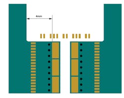
The datasheet also shows the recommended power layout for one side of the LT9890 (the other side “mirrors” it), and it calls out many board and copper-related advisories for optimum performance (Fig. 6).
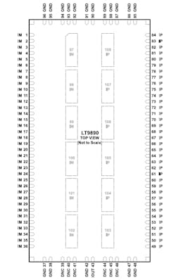
Packaging of the LT9890 is also unusual and unique, also as defined on its 11-page datasheet. Although the device has only a few pin functions, it’s housed in a 108-terminal, 10- × 20- × 2.75-mm LGA package. Why so? Of the 108 connections, 42 are tied together for the positive current input and 42 are for the negative current input (Fig. 7). As we’re talking 150 A here, the physical connecting-copper mass is critical.
Once again, when it comes to many analog-function ICs, it’s like the old saying goes: “Sometimes less—if done right—is actually more.”

