Today, most of the big names in the semiconductor industry are racing into the era of the 3D IC, strapping heterogeneous dies directly on top of each other to improve performance without increasing the power or area of the total package. But adding another dimension to modern chips presents engineers with a wide range of challenges—most of all, managing the heat caused by cramming all of these chiplets so close together.
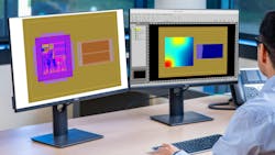
Siemens EDA attempts to beat the heat with the latest product in its Calibre design and verification platform. Called Calibre 3D Thermal, the software is designed for fast and accurate die-level thermal analysis of 3D ICs. By integrating its Simcenter Flotherm physics solver for electronics cooling simulation, the company said it enables chip designers to model, simulate, and analyze the complex thermal effects that exist in these 3D chips.
According to Siemens, it can evaluate the thermal situation from the “package inward,” from separate dies to through silicon vias (TSVs) used for power distribution and die-to-die interconnects linking them. The multiphysics software can create fine-grain power maps of the heat pumped out by all of the components in the package and use them to highlight hot spots and temperature gradients spreading out through the 3D package.
Calibre 3D Thermal stands out from other tools, said Siemens, by giving engineers the ability to run thermal analysis at any point in the chip design process, from the early stages of design exploration to final signoff.
As the monolithic era of the system-on-chip (SoC) ends, thermal analysis becomes one of the most important tools in the engineer’s toolbox. But leaving it to the very end—after the chiplets are assembled in the 2.5D or 3D package—can disrupt the design process. By evaluating thermals inside the package every step of the way, engineers can use Calibre 3D Thermal to identify and fix potential issues before they cause headaches.
“What we’re introducing is the ability to do early feasibility analysis well in advance so you can head off any potential thermal problems much earlier than you might have been able to traditionally,” said Michael White, senior director of physical verification product management for Siemens Calibre. He added that engineers can evaluate the thermal situation even in the middle of floorplanning for cells, blocks, and chips, giving them the ability to test different arrangements of chiplets and other solutions when they still have the flexibility to do so.
Heat: The No. 1 Threat to the Future of 3D Chips
With the scaling of transistors becoming prohibitively costly and the usual performance, power, and area (PPA) gains that comes with every new node slipping, the 3D IC is pivotal to pushing Moore’s Law into the future.
Instead of spreading out all of a SoC’s capabilities on the same slab of silicon, many of the most advanced CPUs, GPUs, and other chips spread them out over distinct heterogenous dies or chiplets, which can cover functions from logic to memory and connectivity. Each of these modular tiles can be built on the best process technology for the job. Thus, you could push out a complex and costly move to a new process node for all of the capabilities you want to put in the package, noted White.
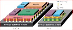
To mimic a SoC without being bound by the reticle limit, these chiplets are bolted together on interposers threaded with die-to-die interconnects or other 2.5D packaging technologies that are current gold standard for AI chips in the data center. To bind these heterogeneous dies even closer together, they can be stacked on top of each other in a 3D package, where microscopic bumps of solder act as die-to-die interconnects and vertical vias distribute power from the ground floor of the package to the chiplets above.
“The traditional reticle limit for how the SoC is manufactured rarely holds enough transistors to be able to handle the demands of AI, and that is only getting worse,” said John Ferguson, who leads 3D-IC product management for Siemens Calibre. On top of that, the latest AI chips are evolving to be even more power-hungry. “The amount of power that is required to do AI is outrageous, and it is growing by huge amounts.”
To make sense of the intricate geometries and material complexities in 3D packages, Siemens and other EDA giants, including Cadence and Ansys, are investing more in multiphysics tools, and specifically thermal-analysis software.
The high density of transistors and large amounts of current consumed by multi-die systems raises the risk of thermal issues. When silicon dies are stacked on top of each other, the heat between them can have trouble slipping out. The heat not only takes a toll on the performance of the transistors, but it could affect the delivery of power and signals, too, along with timing. Siemens said it makes more sense to prevent heat from building up between the dies in the first place before it saps the system’s performance and reliability.
Removing heat from any one chiplet can also impact the thermal situation in other chiplets under or on top of it. The phenomenon—called thermal coupling—may extend to the package, substrate, and the PCB, too.
Feeding power smoothly to the chiplets in the package is a challenge in and of itself. What complicates it is the relationship between power and heat. The thermal and material properties of each die are different, as is the power used by each one, resulting in different heat distributions for every block. It leads to hotspots that can be hard to predict in harsh environments or under dynamic loading conditions.
These chips also have large thermal gradients, since it’s possible to cram more square millimeters of silicon in the package. Moreover, they have a higher risk of physical stress due to varying rates of thermal expansion in different chiplets.
Mapping out the thermal situation is traditionally one of the last stages of the chip design process, since in most cases you can prevent heat by carefully adjusting the widths and spacing of the wires inside the SoC, said Ferguson.
However, binding chips together in 3D is “breaking” the usual approach to thermal analysis, he added. “Once a traditional chip is manufactured, you sort the good dies from the bad. But today, even after you know you have good dies, they may not behave the same in the context of the package as they do [by themselves]—depending on the thermal impacts they can have on each other. So, while you’ve designed every chiplet the best way you know how, you’re left with the question of whether it is actually going to work, and it may not be clear.”
Managing Heat Inside and Outside of 2.5D and 3D Packages
Siemens said Calibre 3D Thermal solves the problem by giving engineers the ability to “shift-left,” meaning that that they can run thermal analysis from the very early stages of the development of chiplets and the 3D IC around them.
“They only need some understanding of the metal layers involved, the rough thermal characteristics of those, and maybe some estimates or guesses of what the power will be for the cells, blocks, or whatever,” said White, adding that customers can use it to, for instance, rule out placing a pair of power-hungry chips too close to each other in the package.
“So, even with that rudimentary information, we can start doing thermal analysis to give you a sense of whether you have a problem—or not. You can do all that when you still have the flexibility to make changes to the floorplan or to the overall design.”
As customers plot out more of the blueprint of the IC—the process technology to be used and the precise power to be consumed by different building blocks in the package—Siemens said 3D Thermal can take it all into account to more accurately analyze the thermal load. The step-by-step approach gives you the ability to adjust the chip’s design to dissipate heat more effectively, add additional vias or wires to avoid thermal hotspots, or apply other fixes.
The multiphysics tool also integrates its Simcenter Flotherm engine to create accurate chiplet-level thermal models for static and/or dynamic simulation of the 2.5D or 3D package. When you know everything that you want to know about heat dissipation inside the package, you can move these thermal models into Flotherm, opening the door to thermal simulation that covers the 3D IC itself out to the package, board, and system level.
“Flotherm can be used for thermal analysis at the system level and the temperatures can be plugged into Calibre as boundary conditions, as in ‘What environment is the package sitting in?’,” said White. “Then, we can take that into account for the thermal analysis inside the package.
“We can run it in reverse, too, so that as we create a highly accurate thermal model of what’s happening within the package, we can plug the model into Flotherm, and then systems engineers can use it for the system-level modeling that they do.”
Siemens said it also outputs all of the information required for thermal impacts to be considered in electrical simulations, giving you the ability to do electro-thermal analysis of the chip design.
Calibre 3D Thermal works with a wide range of other EDA tools, said Siemens, both from its rivals as well as with its suite of software tools, including its recently released Innovator3D platform for 3D chip design.
Check out more of our DAC 2024 coverage. Also, read more articles in the TechXchange: Designing with Chiplets.


