Members can download this article in PDF format.
What you’ll learn:
- What standards address power-supply EMI?
- Methods for mitigation in conducted and radiated EMI.
Electromagnetic interference (EMI) is one of the most damaging and disturbing causes of diminished performance in electronic and electrical devices. Data will be compromised and can even be lost, thus wreaking havoc within most electronic systems.
EMI can be in the form of non-contact radiated (via induction) through the air and/or conducted via direct physical contact, such as with cabling.
Industrial, automotive, and personal-computing applications in electronic systems are fast becoming increasingly interconnected and dense. And the gateway between a product design and development, along with taking that product to market, is to overcome EMI concerns and passing electromagnetic-compatibility (EMC) tests. Electronic companies may encounter serious legal liability with large fines if EMC certification isn’t approved in product testing.
Coupling-Path EMI
One of the main EMI-conducted coupling paths in electronics is through cabling. The European Commission’s EN55022 standard covers conducted EMI frequencies from 150 kHz to 30 MHz.
The primary EMI radiated path in electronics comes from the surrounding air. On this front, EN55022 covers radiated EMI frequencies from 30 MHz to 1 GHz
EMI Challenges in Switching Power Supplies
The power supply for printed circuit boards (PCBs) and integrated circuits (ICs) must adhere to a very careful EMI-based system layout. Spread spectrum/slew-rate control with solid EMI filtering are a must (Fig. 1).
When designing a conventional switching regulator product, we must use advanced or conventional methods to lower the EMI. Neither of these two approaches are perfect, though.
When dealing with low-frequency emissions (<30 MHz) while meeting the necessary standards, designers must be wary of placing a large, passive inductor-capacitor filter in front of the switching power converters. This will lead to a more expensive, less power-dense solution.
If we slow down the switching edges via effective design of the gate driver, designers can mitigate most high-frequency emissions. This will help to reduce EMI in bands greater than 30 MHz thanks to reduced edge rates that will contribute to increased switching losses along with a lower-efficiency solution. Thus, there will be an inherent efficiency and power density tradeoff to achieve lower-EMI solutions.
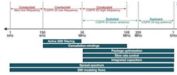
This tradeoff can be resolved, however, leading to the combined benefits of high efficiency, high power density, and lower EMI. Figure 2 shows a few key techniques that are designed into Texas Instruments’s switching controllers and converters.
Methods such as spread spectrum, cancellation windings, active EMI filtering, cutting-edge package innovations, integrated input bypass capacitors, along with solid slew-rate control methodologies are a custom fit to specific frequency bands of interest.
Electromagnetic Compatibility with SMPS
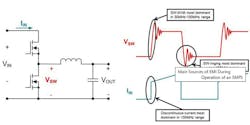
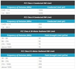
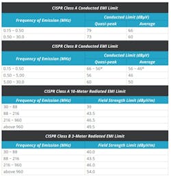
EMC compliance and testing follows an excellent article entitled “Methods of Measurement of Radio-Noise Emissions from Low-Voltage Electrical and Electronic Equipment in the Range of 9 kHz to 40 GHz.” It’s the test procedure as defined in ANSI C63.4-2009. This ANSI standard will not include specific or generic equipment that’s related to products for radiated and conducted emissions. Such limits are specified in pertinent papers by the FCC and CISPR (Figs. 3 and 4).
EMC testing is done with the entire system, not just for the power-supply module, especially in the case of embedded power modules. For external power supplies (like those in standalone power adapters), the complete system must be tested, even though the power adapter may be fully in compliance with regulations.
Mitigation Methods for Conducted and Radiated EMI
One major method for reducing conducted EMI focuses on differential- and common-mode noise separately, since the best remedy will differ for each type of noise. A solution for differential-mode noise can’t eliminate common-mode noise that’s present in the circuitry, and vice versa.
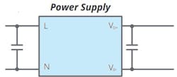
Designers can typically suppress differential-mode noise by employing bypass capacitors between return and power lines in their power-supply design (Fig. 5).
We can suppress radiated EMI by reducing antenna loop area and RF impedance via the power line and return path. Also, design the PCB tracks by making them as wide as possible, and route them in parallel to the return path.
Furthermore, since the impedance of a wire loop is proportional to its area, designers can reduce the area between the power line and its return path. This will further reduce the impedance.
Read more articles in the TechXchanges: Delving into EMI, EMC, and Noise and Power Supply Design.
References
1. “Introduction to EMI: Standards, Causes and Mitigation Techniques,” Yogesh Ramadass, SSZT173.
2. “An overview of conducted EMI specifications for power supplies,” Timothy Hegarty, Texas Instruments 2018.
3. “Simple Solutions for EMI Mitigation at Any Stage of Product Development,” Schaffner, 2023.
4. “Introduction to EMI in power supply designs, High Voltage Seminar, Isolated Gate Drivers,” Bing Lu, Texas Instruments, 2021.
5. “Electromagnetic Compatibility Considerations for Switching Power Supplies,” CUI Inc., 2019.
6. “TI pioneers the industry's first stand-alone active EMI filter ICs, supporting high-density power supply designs,” Texas Instruments, March 20, 2023.
7. “Electromagnetic Compatibility: Challenges, Solutions, and Best Practices for Mitigating EMI in Electronic Systems,” Shaini Garg, Hassan Mohammed Esa Lashkari, Haresh Pokale, 2023 Innovations in Power and Advanced Computing Technologies (i-PACT).
