What you’ll learn:
- How researchers are employing advanced materials and semiconductor techniques to address electro-optical needs.
- How they developed photonic IC (PIC) circuit elements including power couplers, phase shifters, and wavelength-division multiplexing devices using standardized technology.
- How an innovative ultra-low-power design can compensate for thermal drift in wavelength-division-multiplexed (WDM) electro-optical links.
The mutually beneficial relationship between photonics and solid-state processes continues, with photonic IC (PIC) projects and progress in many areas that go far beyond just basic emitters and receptors. It’s a case where use of silicon and other materials opens up new, viable ways to manage photonic signals and exploit their bandwidth potential, while photonics leverages the tremendous knowledge base, experience, and materials of solid-state technology. Two recent and very different examples illustrate the efforts underway as well as the associated advances.
Photonic MEMS Platform
A team of researchers at the University of Sydney has developed a technology to combine optics and MEMS devices in a microchip package. Their photonic MEMS platform builds on imec’s iSiPP50G platform, which can be considered representative for advanced standardized silicon photonics (Fig. 1).
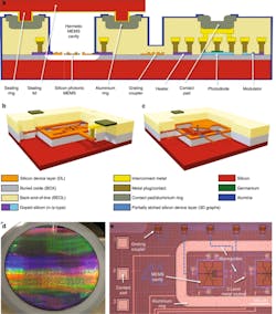
1. The platform is based on imec’s iSiPP50G platform, enhanced with custom post-processing to produce suspended and movable MEMS structures alongside the platform’s standard components and with sealing caps above the MEMS structures to provide protection of the movable MEMS devices. (a) Schematic cross section of the technology platform and 3D perspective views of (b) in-plane and (c) out-of-plane movable devices to visualize conceptually the electrostatic actuators, the optical and electrical routing, as well as grating coupler and metal contact pads, serving as interfaces. (d) Photograph of a 200-mm silicon-photonics wafer before MEMS release post-processing and (e) microscope recording of a representative MEMS device integrated alongside high-performance grating couplers, low-loss waveguides for optical routing, and two metal levels for electrical routing. The final metallization layer serves as a bond pad for wirebonding, as well as an aluminum ring for the wafer-level hermetic sealing process.
It consists of high-performance nano-opto-electromechanical devices fully integrated alongside standard silicon-photonics foundry components. Wafer-level sealing is employed for long-term-reliability, flip-chip bonding to redistribution interposers, and fiber-array attachment is used for optical and electrical interfacing with high port count.
Their demonstration of these photonic IC (PIC) circuit elements includes power couplers, phase shifters, and wavelength-division multiplexing devices using standardized technology. It enables scaling to very large photonic integrated circuits for applications in telecommunications, neuromorphic computing, sensing, programmable photonics, and quantum computing.
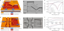
For example, they explored how electrostatically controlled physical displacements of MEMS structures at the microscale and nanoscale can be used for optical power distribution and switching. Their MEMS-based directional coupler allows redirection of the optical power from the input to either output (Fig. 2). A full transfer of optical power at a given operating wavelength between the two coupler branches is accomplished via an out-of-plane displacement of 300 nm.
2. (a) 3D schematic view of an out-of-plane actuated tunable power coupler indicating the input, through, and drop ports as well as the actuator. (b) SEM recording of the released device showing a cleanly suspended and initially well-aligned configuration of the couplers in the unactuated state. (c) Measurement results for the spectral characteristics of the tunable power coupler under dc actuation showing a maximum extinction ratio of 25 dB between the drop and through ports in the unactuated (0 V) state and a maximum extinction ratio of 30 dB in the actuated (27 V) state. The associated 3-dB bandwidth of this device is >30 nm. (d) 3D schematic view of an in-plane actuated photonic 1 × 2 switch with the movable input and two fixed outputs. (e) SEM recording of the released device showing the curved electrodes, stoppers, and suspended waveguides. (f) Measurement results for the spectral characteristics of the device in all three functional states: ON1, OFF, and ON2, wherein the extinction ratio is >23 dB for both ON states and the bandwidth is >70 nm.
The work is fully detailed in their paper “Integrated silicon photonic MEMS” published in Nature’s Microsystems & Nanoengineering. Despite its short title, the paper is very long (22 pages!) and, frankly, challenging to read due to its lengthy sentences and lengthier paragraphs, but it does provide an in-depth presentation.
Ultra-Efficient Temperature-Variation Compensation
In a very different place and application, a team comprised of researchers from Oregon State University and Baylor University developed a way to save energy in the photonic interfaces used in data centers and supercomputers. They devised an ultra-energy-efficient method to compensate for temperature variations that degrade photonic devices.
At present, this is done via components known as “thermal heaters” to fine-tune and thus adjust the working wavelengths of high-speed, electro-optic devices and optimize their performance. While these thermal heaters consume several milliwatts of electricity per device, it adds up very quickly in a given installation, where there may be many thousands of such optical interfaces.
Silicon microring resonators (Si‑MRRs) play essential roles in on‑chip wavelength-division-multiplexing (WDM) systems due to their ultra‑compact size and low energy consumption. However, the resonant wavelength of Si‑MRRs is very sensitive to temperature fluctuations and fabrication process variation. To compensate for this shift, each Si‑MRR in the WDM system requires precise wavelength control by free-carrier injection using PIN diodes or thermal heaters that consume power.
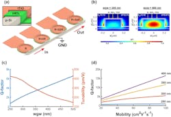
The team has demonstrated an alternative: gate‑tuning on‑chip WDM with large wavelength coverage for the entire channel spacing using a Si‑MRR array driven by high-mobility, titanium‑doped indium oxide (ITiO) gates. Their on-chip WDM filters consist of four cascaded, tunable Si-MRRs of different radii with metal–oxide semiconductor (MOS) gates formed by a high-mobility, transparent conductive oxide (TCO), which show much larger electro-optic (E-O) efficiencies than reversed PN junctions (Fig. 3).
3. (a) 3D schematic of the on-chip WDM filters consisting of four cascaded tunable Si-MRRs with different radii. Inset: zoom-in view of microring waveguide with ITiO/HfO2/Si MOS capacitor. (b) Simulated mode profiles in the active region with waveguide widths of 300 and 400 nm, respectively. (c) Simulated Q-factor (blue) and tunability (orange) versus waveguide widths by assuming that the gate material has a carrier concentration of 3 × 10¹⁹/cm and mobility of 25 cm2/V-sec in the simulation. (d) Simulated Q-factor as a function of mobility with different waveguide widths, assuming that the bent Si waveguide has a radius of 8 μm and a height of 250 nm with a 50-nm slab in the simulation.
As a result, it can provide a large wavelength-tuning range with a low gate voltage and negligible power consumption. They demonstrated that an individual tunable Si-MRR could achieve an extremely high wavelength tunability of 589 pm/V (0.050 V-cm) with a high quality factor (Q-factor) of 5,200. [Note that the Q-factor of previous attempts was limited to 1,000 due to the low carrier mobility, which in turn caused a high optical absorption. Such a low Q-factor restricts the channel density of the WDM module.]
Each channel in the fabricated on-chip WDM filters could be independently tuned by applying gate bias, achieving continuous wavelength coverage from 1,543 to 1,548 nm with near-zero power consumption. Further, the gate biases could compensate for fabrication errors and so maintain uniform channel spacing of the four cascaded Si-MRRs. The MOS-driven silicon-photonic devices can be heterogeneously integrated with other semiconductor materials such as III–V compound semiconductors and TCOs to achieve even better E-O efficiency.
In the fabricated on-chip WDM filters and testing setup, the input and output fibers have a tilt angle of 10 degrees, and the light is coupled into and out from the on-chip WDM filters through the grating couplers (Fig. 4).
4. (a) Optical microscope image of the fabricated on-chip WDM filters consisting of four cascaded tunable Si-MRRs and testing setup. (b) Zoom-in view of the individual tunable Si-MRR of the on-chip WDM filters. The dashed line highlights the ITiO gate. (c) The simulated carrier concentration (Nc), refractive index (n), and extinction coefficient (k) distributions with different applied biases at the ITiO/HfO2 and the Si/HfO2 interfaces.
The GND probe serves as the common ground for the on-chip WDM filters, and each channel is independently tuned using the gate bias through the single probe. The figure also shows the zoom-in view of the on-chip WDM filters, and the ITiO gate covers the active region of each Si-MRR. When the negative bias is applied, the accumulation of free carriers induces the change of refractive index and optical absorption originating from ITiO/HfO2 and Si/HfO2 interfaces.
The work is described in their brief (7 pages) yet very readable paper “On‑chip wavelength division multiplexing filters using extremely efficient gate‑driven silicon microring resonator array,” published in Nature Scientific Reports.


