What you’ll learn:
- The growing demand for smaller, more power-efficient, and higher-performing ICs.
- The need to address advanced architectures like chiplets and stackable dies.
- How the Tessent test access architecture speeds and simplifies chip-scale test.
The pressure to increase chip density has caused designers to leapfrog Moore’s Law and leverage other technologies beyond sheer feature size to address it. Since Gordon E. Moore, co-founder of Intel, predicted that the number of transistors per square inch on an IC would approximately double every year, the industry has managed to keep up.
However, that ability is fading in the face of more and more challenging physics. There are other ways, though, to address chip circuit density—namely, scalable tiled and stacked chip integration.
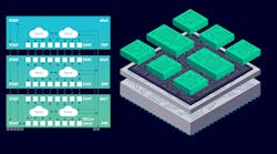
Currently referred to as 2.5D, 3D, and 5.5D IC architectures, these advanced approaches will extend Moore’s Law going forward, but will present significant challenges for IC test and design-for-test (DFT) teams (Fig. 1). The side-by-side 2.5D solution also is referred to as a “chiplet” architecture, and it represents the first generation of these technologies. 3D systems involve stacking chiplets, and a 5.5D solution employs both side-by-side and stacked chiplets.
Integrating multiple chiplets into a single package creates a powerful device with a high transistor count, reducing cost and maximizing performance. However, integrating these chip-scale systems puts pressure on the packaging, die integration, and pad patterning. Siemens EDA recently launched what it says is the first solution to dramatically speed and simplify critical design-for-test (DFT) tasks for next-generation ICs based on those 2.5D, 3D, and 5.5D architectures.
The Tessent Multi-die software solution helps speed and simplify those critical DFT tasks. Working in conjunction with Siemens’ Tessent TestKompress Streaming Scan Network software along with Tessent IJTAG software, the solution optimizes DFT test resources for each block without worries over impacting the rest of the design. This streamlines DFT planning and implementation for these advanced chip architectures, quickly enabling the creation of IEEE 1838-compliant hardware.
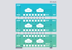
Beyond enabling comprehensive tests for 2.5D, 3D, and 5.5D IC designs, the Tessent Multi-die solution can generate die-to-die interconnect patterns, allowing for package-level testing with boundary scan description language (Fig. 2).
The solution supports integration of flexible-parallel-port (FPP) technology, leveraging the packetized data-delivery capabilities of Siemens’ Tessent TestKompress Streaming Scan Network software. The network decouples core-level DFT requirements from the chip-level test-delivery resources, enabling an improved DFT flow that simplifies DFT planning and implementation, reducing test time up to 4X.


