This article is part of the TechXchange: Cool Designs.
What you’ll learn:
- The thermal problem the researchers seek to mitigate.
- The two-stage, unusual technique they investigated and tested.
- The multifaceted implications and results of their approach.
Keeping hot components and especially power devices within their allowed maximum thermal limits is an ever-present design challenge. Among the many techniques employed are top-side heatsinks, thermal interface pads or diamond films, bottom-side dissipation via the PCB, heat spreaders, heat pipes, and more—coupled with active or passive cooling using convection, conduction, and even radiation.
The challenge increases when other warm sources are nearby: Cooling options depend greatly on the temperature differential between the heat source and the place called “away” to which that undesired heat is being transferred.
Now, a team at the Grainger College of Engineering of the University of Illinois Urbana-Champaign (UIUC), working with the University of California at Berkeley (UCB), has devised an unconventional scheme that definitely helps conduct away from those hot components, but with some implementation and usage complications.
Creating the Coating
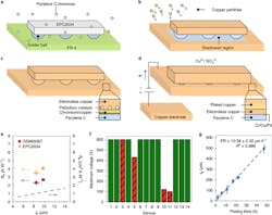
Their approach first coats the devices with an electrical insulating layer of parylene C, widely used for conformal coating of fully loaded circuit boards to provide protection against moisture and corrosive gases.1,2,3,4 Subsequently, using successive depositions with thermal evaporation, electroless plating, and electroplating, a conformal copper coating is monolithically grown on the parylene C (Fig. 1).
1. Cu-coated heat spreader fabrication: (a) Schematic showing the coating of GaN devices and PCBs with a layer of parylene C for electrical insulation. (b) Schematic of the deposition of a 20-nm-thick Cr layer followed by a 50-nm-thick Cu layer via PVD. (c) Schematic of the electroless deposition of Cu to cover the shadowed regions underneath the devices and create a continuous Cu film that can drive electrical current from FR-4 to the top of the device. (d) Schematic showing further growth of Cu using dc. Cu electroplating. (e) Calculated thermal resistance RP of parylene C and specific thermal resistance based on the measured thickness tP of parylene C. (f) Maximum voltage drop applied across the parylene C layer for different devices tested. The solid green bars and shaded red bars correspond to layers that passed (leakage current <1 µA) and failed (leakage current >1 µA) the voltage test, respectively. (g) Cu-coating thickness as a function of electroplating time. (Credit: UIUC)
The conformal copper reaches underneath the devices to create contact with heat-generating regions, then provides thermal-dissipation routes along all surfaces and leads of the device package. This allows the copper to be close to the heat-generating elements, eliminating the need for thermal interface materials and providing improved cooling performance compared with existing technologies.
Test Results
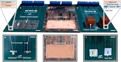
They tested performance using both air and water cooling with two different GaN power transistors: a top-cooled GS66508T surface-mount device (SMD) and a top-cooled EPC2034 ball-grid-array (BGA) device (Figs. 2 and 3). The team showed that it can be used in systems operating at up to 600 V.
2. Photographs of the tested configurations (a-c), Photographs of 4.8 cm × 2.5 cm 70-µm-thick solder-coated Cu-plane heat spreader: (a) Cu-coated heat spreader and (b,c) pair of 1.4- × 1.4- × 1.4-cm³ Cu heatsinks. The insets show the schematic of the cross-sectional material stackup of the solder-coated Cu plane (top left) and Cu heatsinks (top right). (d) Custom PCBs having two GaN power transistors: a top-cooled SMD from GaN Systems (GS66508T) and a top-cooled BGA device from Efficient Power Conversion (EPC2034). (e) Top-view photograph of the 5.4- × 2.5-cm Cu-coated heat spreader. (f) To ensure good thermal contact between the GaN devices and Cu heatsinks, layers of gap filler were added, followed by a thermal paste. (All scale bars correspond to 1 cm.) (Credit: UIUC)
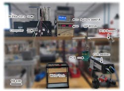
3. Photograph of the experimental setup that includes a PXIe-1073 chassis and TB-4300 Module (National Instruments) data-acquisition system (DAQ), a computer, a water tank for the quiescent water experiments, a printed-circuit-board (PCB) sample with its support, a 34461A digital multimeter (DMM) (Agilent), a 6033A dc power supply (HP), and a A655sc camera (FLIR Systems). (Credit: UIUC)
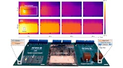
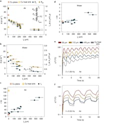
Among their many test results, they found a low junction-to-ambient specific thermal resistance of 2.3 cm2-K/W– in quiescent air and 0.7 cm2-K/W in quiescent water (Fig. 4).
4. Thermal performance of EPC2034 monolithically integrated with copper: (a,b) Thermal resistance (R, left axis) and specific thermal resistance (R″, right axis) as a function of Cu coating thickness (ts) for the (a) air-cooled EPC2034 GaN device and (b) water-immersion-cooled EPC2034 GaN device. TC in the inset corresponds to the place of the thermocouple in the thermal resistor network. TJ, Tamb, and RJC in the inset correspond to the junction temperature of the device, ambient temperature of the fluid, and junction-to-case thermal resistance of the device, respectively. (c,d) Time constant (τ) as a function of Cu coating thickness (ts) for the (c) air-cooled EPC2034 GaN device and (d) water-immersion-cooled EPC2034 GaN device. (e,f) Temperature-swing (ΔT = Ts – Tamb) response as a function of time for the air-cooled EPC2034 GaN device with the Cu heatsink, 55-µm-thick Cu coating, 172-µm-thick Cu coating, and 476-µm-thick Cu coating at a pulsed heat load of (e) 1.00 Hz and (f) 0.33 Hz. (Credit: UIUC)
Tarek Gebrael, the lead author and a UIUC Ph.D. student in mechanical engineering, noted the three benefits of this approach: the primary material used is copper, which is relatively inexpensive; the copper coating "engulfs" the device entirely and covers all exposed surfaces, so no heat-producing regions are neglected; and there’s no need for any thermal interface material as the device and copper heat spreader are essentially one piece, avoiding use of a heat sink.
Co-author Nenad Miljkovic, an associate professor of mechanical science and engineering at UIUC and Gebrael's advisor, noted, "This technology bridges two separate thermal-management approaches: near-junction device-level cooling, and board-level heat spreading.”
Added Gabrael, “In our study, we compared our coatings to standard heatsinking methods, and this translates to much higher power per unit volume. We were able to demonstrate a 740% increase in the power per unit volume.”
What's the Verdict?
My view is that this impressive claim, while mathematically true, is partially due to careful use of numbers with the much-smaller denominator, which is due to the extreme thinness of the copper coating. Interestingly, there are some comments on this paper and its claimed benefits, including some highly negative ones at an Ars Technica forum.5 Further, the authors also don’t address the practical implications of such all-encompassing conformal conductive coating on product test, use, or repair, yet most products must balance more-efficient cooling with these other factors.
The work is presented in their brief paper “High-efficiency cooling via the monolithic integration of copper on electronic devices” published in Nature, along with a 44-page Supplementary Information file. The latter contains extensive details on the procedure, thermal and mechanical modeling and simulation, tables of results, and much more.
References
1. Vertical Solutions Inc., “What is Parylene Coating?”
2. University of Michigan LNF Wiki, “Parylene C”
3. Specialty Coating Systems Inc., “SCS Parylene Properties”
4. Specialty Coating Systems Inc., “Parylene Deposition Process”
5. Ars Technica Open Forum. “High-efficiency cooling via the monolithic integration of copper on electronic devices”
