This video is part of TechXchange: Chiplets - Electronic Design Automation Insights and TechXchange Talks.
AMD has completed its acquisition of Xilinx, and its complementary chip-packaging technology is allowing AMD to integrate heterogeneous chiplets into a single package. This trend has been growing for some time because it allows components built with different levels of silicon processes to be combined into a single unit. It's been used to connect high bandwidth memory (HBM) to GPUs and CPUs.
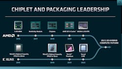
A number of approaches can be used from silicon interposers to elevated-fanout-bridge (EFB) connection. Mark Papermaster, CTO at AMD, talks about (in the video above) the company's new Zen 4 CPU chiplet as well as some of the chip-level interconnects like EFB being used by AMD/Xilinx in current and future chips (Fig. 1).
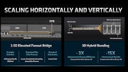
EFB is a lower overhead technique than a silicon interposer. This is more akin to using a jumper rather than a full PCB at the module level, except that an EFB often has hundreds of connections (Fig. 2). Both tend to be referred to as 2.5D connections, since chiplets are adjacent versus the 3D stacking found in memory chips like HBM RAM and flash-memory stacks.
The 3D hybrid bonding that Mark covers is a way to stack different chiplets, but a copper-to-copper connection was used instead of the silicon/metal connections. It's very energy-efficient and provides high-density, low-latency connections. This hybrid 3D technology is already employed by AMD in some of its current offerings.
Foundries like TSMC and GlobalFoundries are supporting 2.5D and 3D technologies. They're required to take advantage of other high-density technologies like HBM that use through silicon vias (TSV) to implement their 3D stacking.
See more articles/videos in TechXchange: Chiplets - Electronic Design Automation Insights and TechXchange Talks.


