Applied Materials rolled out a semiconductor fab tool this month that gives its a new way to engineer copper interconnects in advanced logic chips, solving a stumbling block to future 3-nanometer nodes.
As the semiconductor industry races to roll out smaller and faster chips with more energy efficiency, the focus has largely been on scaling the transistors that act as tiny switches on chips. But the chips also require increasingly sprawling grids of interconnects to link the transistors together. Today, a state-of-the-art 5-nm mobile processor packs more than 10 billion transistors covered by a canopy of tens of billions of interconnects of varying dimensions, stacked in more than 15 layers.
While scaling the transistors translates to more performance (smaller transistors mean more of the infinitesimal switches can be packed on the die), the opposite occurs with interconnect wires, which are formed by filling tiny trenches carved out of the silicon slab with copper. The smaller the wire, the higher its electrical resistance. That saps performance and power efficiency in advanced logic chips.
But as the semiconductor industry moves to more advanced nodes, the interconnects in chips are one of the leading culprits of power waste, heat buildup, and signal delays that hamper the performance of chips. Left unchecked, the resistance of the chip's interconnects would increase by a factor of 10 from 7-nm to the 3-nm nodes. That would wipe out any of the performance gains from shrinking transistors.
The Santa Clara, California-based company said the new tool—called the Endura Copper Barrier Seed system—resolves part of the resistance problem, improving the performance and power efficiency of advanced logic chips. Applied Materials, the world's largest semiconductor gear vendor, said that the wiring tool opens the door for fabs to build chips based on 3-nm and possibly more advanced nodes.
Applied Materials, which sells fab tools to Intel, Samsung, TSMC, and other chip-manufacturing giants, said that the system could be used to scale the interconnect wires in chips to 15 nanometers or about 1/2000 the width of a human hair. The Silicon Valley vendor said using the Endura Copper Barrier Seed tool reduces interconnect resistance by 50%, giving the copper wires in computer processors based on the 3-nm node around the same overall resistance as the most advanced 5-nm chips available today.
“A smartphone chip has tens of billions of copper interconnects, and the wiring already consumes up to a third of the chip’s power,” said Prabu Raja, senior vice president of the semiconductor business at Applied, in a statement. “Integrating multiple process technologies in vacuum allows us to re-engineer materials and structures so that consumers can have more capable devices and longer battery lives."
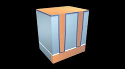
Today, interconnects consist of two core building blocks, including metal "lines"—tiny trenches carved out of insulating layers that supply current within the same floor of copper wiring—and "vias"—deeper grooves cut into the interconnect lines that connect one stack of copper wires to another in advanced logic chips. The interconnects are formed layer by layer by filling these tiny canals with copper (Fig. 1).
But as the semiconductor industry moves to more advanced process nodes, the width and length—the "pitch"—of the interconnects also shrink. The resistance rises, requiring chips to consume more power to force current through smaller wires, resulting in higher power dissipation and, in turn, creating more heat buildup. Higher resistance also means that it takes longer for signals to travel the same distance.
Furthermore, these smaller copper wires are more vulnerable to the impact of "electro-migration." As current rushes through the ultra-thin wires, it can shake loose copper atoms, resulting in microscopic gaps, called voids, that can cause short circuits and cause permanent damage. The solution is to coat the sides of the copper-filled trenches with very thin films of other materials, such as tantalum and cobalt.
The existing production process starts by removing residues and cleaning out the trenches and vias carved in the insulating layers. What follows is a process called atomic layer deposition (ALD), which evenly coats the grooves in the interconnect with a tantalum-based material. The tantalum acts as a "barrier" to protect the copper from unintended contact with the insulating layers. The second phase uses chemical vapor deposition (CVD) to cover the walls with cobalt to encapsulate the copper wire.
The purpose of the cobalt—what industry insiders call the "liner"—is to prevent the copper wires from peeling off the walls of the interconnect, which can lead to gaps, voids, or other catastrophic defects.
Together, the tantalum and cobalt create a sort of mold for the copper wires that fill the interconnect. The copper wires are deposited into the remaining space using another process called "copper reflow," which uses physical vapor deposition (PVD) to blanket copper on the surface of the interconnect with copper. The copper is then heated so that it flows down into the interconnect, forming the final wire.
The problem Applied Materials is trying to address with the new tool is that when current flows down through the interconnect via to other levels of copper wiring, it is forced to push through the tantalum barrier, which has higher resistance than the copper wires. Applied Materials said the interface where the via contacts other floors of copper wiring is the largest factor in the overall resistance of the via.
The other issue is that even as the copper wires in the interconnect have continued to scale down, the thickness of the tantalum has not. That leaves less space for electricity-conducting copper in the via.
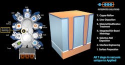
Applied Materials said that the Endura Copper Barrier Seed system can create interconnects without the tantalum lining the base of the interconnect. The tool uses more advanced "selective" deposition (ALD) to only coat the walls of the interconnect with tantalum instead of blanketing the trenches and vias evenly. That increases the volume of copper wire in the interconnect, further reducing resistance.
Applied Materials said the tool also features its latest copper reflow technology that fills in the furrows without gaps or voids that can hurt the performance of advanced logic chips. Applied Materials said that its Endura Copper Barrier Seed tool can reduce resistance where the via comes in contact with other copper wires by up to 50%, which adds up when it comes to the tens of billions of vias inside modern logic chips.
Because all these materials can be damaged when exposed to the air, the whole process needs to take place within a vacuum-sealed processing chamber. Applied Materials said the Endura Copper Barrier Seed system can send shimmering slabs of silicon through all the phases of the wiring production process under vacuum: surface treatment, interface engineering, ALD, PVD, CVD, copper reflow, as well as metrology.
While Intel and others in the semiconductor industry are contemplating other metals, including cobalt, to replace copper wires, which have countless technological handicaps, Applied Materials said that its latest tool would allow fabs to continue using copper interconnects in chips for the foreseeable future. It is already being used by major foundry logic customers around the world, according to the company.


