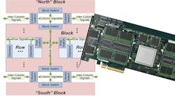
Micron’s Automata Processor (AP) uses a unique parallel processing technique that exploits the company’s memory technology (Fig. 1). The parallel processor is similar to an FPGA and a content addressable memory (CAM), but it is designed to handle stream-processing tasks in parallel. It is well suited for applications ranging from regular expression processing used in deep packet inspection (DPI) and elsewhere to rule-based systems that have been limited in scope because of the processing overhead.
This file type includes high resolution graphics and schematics when applicable.
Related Articles
- Dev Tools Target Parallel Processing
- Tool Delivers Parallel Programming Recipes
- How To Put OpenCL Into An FPGA
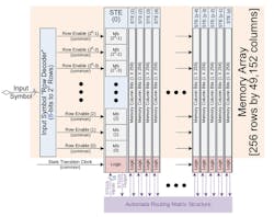
Processing is grouped into blocks of 256 state transition elements (STEs). The same input information is provided to each STE that also contains a value that’s compared to the input. There is additional logic in each STE so it knows when it is activated.
Each cycle starts with data being provided to the system. Each active STE compares the data to their value in parallel and generates an output that is sent to activate one or more STEs. There are 49,152 STEs in the initial implementation. Up to 6144 can be terminal events.
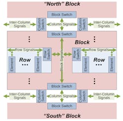
Routing to the next STE can occur within the block (Fig. 2). Signals also can be routed to the block’s nearest neighbors, enabling the construction of more complex systems. Propagation to the nearest neighbor is within a single cycle, so events can be pushed out from a central STE to remote blocks.
The routing of information and its configuration is similar to an FPGA in that a static path is set up between elements. Unlike an FPGA, the Automata Processor has a more limited and regular computational structure. It would not be used to create processors or general boolean logic like an FPGA, but it can handle matching chores and provide significantly more memory with more processing efficiently for many applications compared to an FPGA. In fact, simulating the Automata Processor in an FPGA is impractical on a large scale.
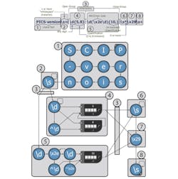
A CAM supports spatial matching but not temporal matching. The Automata Processor can do both, allowing it to process regular expressions (Fig. 3). The example highlights a single expression implemented via linked STEs. A system would consist of possibly hundreds to thousands of expressions operating in parallel.
The logical view of the process makes more sense and matches the kind of development tools available for the system. The system uses an approach similar to FPGAs with a high-level, logical programming language called the Automata Network Markup Language (ANML) that is then compiled and loaded into the configuration portion of the STEs. It essentially includes an STE’s value and target STE, which are accessed as normal memory elements, allowing the system to appear as regular memory with hidden functionality.
The software tools provide simulation support, including animated operation as well as parallel debugging and trace support. The tools and techniques will be different from those used in conventional debugging, so developers will need to get up to speed to address the AP architecture and applications.
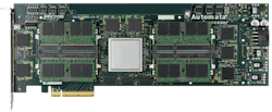
The first implementation of the Automata Processor will be on a dual-inline memory module (DIMM) that is DDR3 compatible (Fig. 4). The DIMM includes eight AP chips. All eight APs can be used together, or they can be partitioned such as two sets of four APs. The first PCI Express board implementation will include up to 48 APs (Fig. 5).
The Automata Processor takes a new approach to parallel processing. Like GPUs, they have a focus where the capability can provide orders of magnitude improvement over conventional parallel processing methodologies. The initial implementation targets a PCI Express host, but the architecture is amenable to other configurations such as pairing an AP with a microcontroller or an FPGA. As with GPUs, it will take some time for developers to take full advantage of the architecture, and new methods will be discovered and employed.
