This article is part of the TechXchange: Addressing Chip Verification Challenges.
What you'll learn:
- Designing the hardware-software interface.
- Dealing with "bytes enables" in RTL verification.
- Automating the HSI design process across the entire dev team.
The hardware-software interface (HSI) holds an important role in chip design, bridging the physical hardware and its software counterpart. It provides integration and performance optimization in complex system-on-chip (SoC) designs. However, issues can still arise with compatibility, timing, synchronization, testing, debugging, performance optimization, reliability, and power management.
Hardware and software engineers seek to balance HSI challenges and requirements. Engineering groups have differing terminologies, though, adding another level of complexity to the project. Consequently, each group of engineers has their own unique areas of concern.
A Complex Challenge for RTL Architects
As the adage goes, "It doesn't ship until the device driver works." This means that designers should collaborate with register-transfer-level (RTL) verification and software teams whenever possible. The architects often find themselves at the forefront of this challenge. The verification process usually requires more time and attention than it took to develop the RTL itself (Fig. 1).
Software development consistently demands that more features be integrated into hardware. An example is the frequent request for "byte enables"—a feature that software developers believe enhances performance and throughput. This technique serves as a mechanism through which software divides operations into more manageable segments within registers by accessing registers in smaller pieces than the whole register.
However, byte enables can make hardware more complex and confusing. Although supported by many bus protocols, byte enables requires tremendous work for the verification team and the RTL designers, resulting in more time to complete the project.
The complexity of this task escalates when fields span multiple bytes, or straddle byte boundaries when there are incomplete bytes. For those operating in a chip design environment, byte enables is a feature that requires a significant amount of time. Checking and designing RTL registers requires a considerable investment, not to mention the challenges of using various bus protocols like AMBA AXI, AMBA APB, and even custom protocols at times.
RTL architects are also in charge of creating up-to-date documentation of the HSI to be shared across the teams. This documentation is essential to help others understand the operation and usage of each field, and thus have it validated correctly by the verification team as well as the right driver being created by the software team according to the latest changes. As the project shifts left, they need to make sure the documentation around the HSI is accurate and up-to-date.
Verification Engineer's Crucial Role in Functional Accuracy
A verification engineer’s job involves ensuring the functionality of the RTL provided by the hardware team before it goes to the software team. This task can be challenging, especially given the wide range of possible design variations and the extensive state space of designs. Even validating memories, registers, and fields within a design can be difficult. Moreover, the complexity increases as more features are incorporated.
In addition to byte enables and the substantial work to verify all of the different byte combinations work correctly, another issue arises from the mixing of different fields within registers. RTL architects often merge various fields into a single register to conserve space. This practice results in registers that combine different access types, including read-only, write-one-clear, and other access methodologies.
Mixing access types in the same register complicates the verification process. Efficiency and swiftness are key to ensuring the project proceeds smoothly through the verification phase and gets to the software developers on time.
Optimizing HSI With Firmware Driver Developers
In chip development, firmware driver developers are tasked with writing the device drivers. This team is typically at the end of the development process because their work can’t begin until the verification and hardware teams complete their tasks. While a shift-left movement is growing to expedite this process, a solution remains a work in progress. Until then, firmware developers stand as a bottleneck—a challenge they want to minimize.
To help facilitate a smoother process, driver developers advocate for implementing array structures within hardware designs. Arrays simplify software development, enabling straightforward access to registers and memory. Without arrays, the software team must manually create functions and macros to interact with each register individually.
By adopting array structures, these functions can rely on simple mathematical indexing, streamlining the entire process. However, not all hardware engineers are proficient at creating array structures.
Automating All Facets of HSI Design
One solution to address the challenges and different requirements across the design teams is CSRCompiler technology. Arteris developed a scalable and robust methodology to automate all aspects of HSI design, verification, firmware, and documentation.
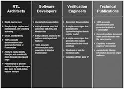
From a single source, the entire design team has access to the address map information. The information is provided in many views. Each team member can retrieve the information in the format required (Fig. 2).
- The RTL designer is provided with the synthesizable RTL implementation of the address map, including the bus interface with address decode, the registers, and the fields.
- The design verification engineer can access header files or classes used to access the fields in a verification environment.
- The software engineer is supplied with the header files and hardware abstraction layer to provide driver access to the registers.
- For the technical writing team, there’s a detailed reference document for internal and external distribution with tables for the addresses, register layout, and field function.
- Automatically generated dynamic web pages have the address map information and there are automatically generated accurate HSI collaterals.
Simplifying the Process for the Design Teams
The ever-evolving landscape of semiconductor chip design necessitates effective communication between design teams. The HSI serves as the bridge, and while challenges persist due to differing languages and requirements, tools like the CSRCompiler help simplify the process.
The methodology automatically documents changes across entire functional teams to deliver a reliable, up-to-date specification. It provides a single-source specification for register and memory-map information, fully configured for all teams in the formats and views they require.
Read more articles in the TechXchange: Addressing Chip Verification Challenges.


