What you’ll learn:
- What is an analog front-end (AFE)?
- Why use an AFE?
- AFE tradeoffs in energy-meter design.
Sensors provide analog signals that need to be converted to digital values via analog-to-digital converters (ADCs). The challenge is the sensitivity of the ADCs. Typically, an analog front-end (AFE) is needed to make the sensor’s signal suitable for conversion.
What’s an Analog Front-End (AFE)?
Fundamentally, any device that performs an analog interface function for a separate digital controller could be called an analog front-end (AFE). Even something as simple as an operational amplifier (op amp) arguably does the job.
In practice, the term is usually reserved for a more integrated device, combining multiple functions or multiple channels to create a comprehensive interface for a specific application. Most contain a combination of one or more programmable gain amplifiers (PGAs), ADCs, and digital interfaces (SPI, I2C, or similar standards).
The amplifiers condition the analog signals, the ADCs transform them to a digital representation, and the interface communicates it to another device on the board. This simple-sounding operation is critical in most electronics, but the silicon implementations behind it can be very difficult.
Capabilities of AFEs: What Does an AFE Do?
Signal conditioning is an application-specific problem, so AFEs are often designed with a single application in mind. The details may vary, but the theme is the same: Take the specialized analog circuitry required for a function and put it in one integrated device to work with a digital controller. Both the AFE and digital controller can be selected separately based on what’s ideal for the circuit requirements.
In one case, the signal chain may start with an antenna, and the AFE may need to bandpass-filter the signal of interest, gain it up, and center it in the range for an analog-to-digital conversion. It would then perform that conversion, serialize the result, and send it by SPI to a digital signal processor (DSP).
In a different application, the input may be a sensor, with specific voltage and current capabilities that aren’t compatible with a typical digital GPIO input. In this case, the AFE could need to accept the sensor output on a low capacitance input or at an unusual voltage range, filter it, scale it, convert it to a digital representation, and relay that information to a microcontroller (MCU) using an I2C interface.
Some applications may require galvanic isolation between the system inputs and the digital processor making the decision, adding a different requirement to the AFE signal chain. In every case, the AFE role is the same: Analog inputs are turned into digital outputs.
Benefits of AFE-Based Solutions: Why Use an AFE?
The system benefits of this approach aren’t necessarily obvious. From a system designer perspective, a single-chip solution will often look like a quicker implementation, and integrated solutions do exist. Some MCUs or digital signal controllers (DSCs) are perfectly capable of being their own analog-front-end using integrated components.
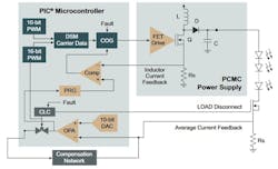
One example is a PIC16F1769, an 8-bit MCU with a 12-channel, 10-bit ADC and two 10-bit digital-to-analog converters (DACs). This device was obviously intended to do its own analog interfacing, and the part can control a switch-mode power supply for an LED drive with all of the analog control signals routed directly into the MCU. Only the power FET drive output signal needs to be run through a MOSFET driver. For this circuit, no AFE was required, and the external analog discrete components were minimal (Fig. 1).
However, in many systems, there’s no MCU or DSP that can directly handle the analog signals because it would be cost-prohibitive to try to make one. To understand this, think about how these devices are designed and manufactured.
Analog chips are manufactured on analog wafer process technologies. Fabs and foundries create technologies that may not be the smallest or the fastest, but they have both CMOS and bipolar transistors, precise resistors, and capacitors that can be matched to each other. They also possess higher voltage withstand capabilities on specialized transistors, and isolation wells or SOI layers to prevent noise propagation between circuits. These features increase the wafer cost but benefit the analog structures on the chip with improved performance or smaller area requirements.
Such analog characteristics are generally independent of the process lithography, e.g., size. For instance, the area required to create a matched resistor network may depend more on the resistor material available than the smallest drawable line—a larger geometry thin-film resistor may outperform a small lithography polysilicon resistor in accuracy, matching, and silicon area required.
Digital devices, on the other hand, benefit from the smallest possible transistor and have historically scaled with Moore’s Law. Each generation outperforms its larger predecessor on a cost of performance basis.
Sometimes, do-it-all wafer technologies can make system-on-chip (SoC) solutions for a specific application, but this approach may suffer from both the high layer count of analog wafer processes and the high per-layer cost of advanced digital nodes. As a result, often the ‘best’ system solutions are achieved with specialized die, a separate controller, and analog front-end.
Tradeoffs in Energy-Meter Designs
Energy-metering applications can illustrate this tradeoff. Solutions for that application are wide-ranging, from integrated SoCs and multichip approaches using AFEs to discrete component implementations.
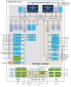
At the top of the food chain, something like an ATSAM4CM (Fig. 2) will include a dual-core Arm Cortex-M4 processor, combined with all of the relevant analog circuitry to produce a class 0.2 utility meter (basically, a 0.2% accurate measurement). It embeds public key cryptography to prevent anyone from hacking the meter, and existing software libraries for that SoC can speed up product development. If the integrated features are all required, this is an excellent solution, and it comes in a 14- × 14-mm package.
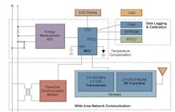
However, a well-designed circuit designed using a standalone MCP3910 (analog front-end for metering applications) can produce a class 0.1 meter (0.1% accurate meter). The device sits in a significantly smaller 4- x 4-mm package (Fig. 3).
Comparting the specifications on those two devices: the temperature drift on the reference in the AFE chip is lower (9 ppm/°C vs. 10 ppm/°C), the resolution on the ADC is higher (24 bits instead of 20 bits), the dynamic range on the ADC is wider (112 dB vs. 102 dB), and the gain range on the integrated PGAs is wider (up to 32X vs. up to 8X). In every analog-specification, the dedicated AFE chip outperformed the SoC device.
This obviously isn’t a fair comparison, as the standalone AFE would need an additional microcontroller to match the capabilities in the SoC, and the multichip solution has some additional board-level design requirements that the SoC would avoid (like the security implementation). While it may be less accurate, some applications will be completely satisfied with the analog capabilities of the SoC, and the ease provided by the integration may outweigh any performance improvement from a dedicated analog AFE.
Discrete Solutions: When There’s No AFE
In addition to those integration tradeoffs, many applications benefit from or require completely discrete solutions for signal conditioning. One example is an on-board charging (OBC) circuit. This is a common module in electric vehicles that takes power from a typical residential 120- or 230-V AC outlet and converts that to DC to recharge the battery.
That’s separate from, and lower power than, a charge pile (fast-charging station) that provides DC power directly to the battery charging circuit. However, despite being “lower power,” a typical module converts more than 10 kW of AC power to a ~800-V DC output. Sometimes, it’s even desirable to create OBC modules capable of bidirectional power conversion. Therefore, the battery energy can be used to provide AC power back to the residence, which significantly complicates the power conversion.
The input AC voltage and battery voltage need to be properly isolated from each other, and from everything else as well. Still, the controller requires measurements on these analog signals to provide regulated outputs. The input voltage, output voltage, current, and temperature all must be measured and the sensors need to be galvanically isolated.
In the case of the Microchip reference design (Fig. 4) for this application, there’s a measurement circuit that uses resistive dividers and amplifiers to condition the voltage signal for a DSP, on a physically separate board from the other control circuitry. In addition, optoisolators are used on the digital communications between the measurement board and the control circuitry.
The current-sense circuit is also in a different place, directly in the current path on the main circuit board. Even the communication out of the module is implemented with an isolated CAN bus. In this application, it would be very difficult to make an AFE to handle such signal conditioning—the voltages are high enough to require physical separation and the isolation capability is difficult to integrate.
AFEs Strike a Balance Between the Extremes
There’s undoubtedly a trend in the semiconductor industry toward increasing levels of integration. For many applications, SoC solutions can be cost-effective or easy to design with. In other cases, system designers may prefer to use discrete components and manage every signal at every stage across the board. In between those two extremes, many applications can apply AFE-based implementations that offer a balance of performance, size, and flexibility.

