Members can download this article in PDF format.
What you'll learn:
- How fluorescence detection is used for in vitro diagnostics.
- Requirements for building an effective fluorescence-detection system.
- Why an integrated optical front-end receiver makes the most sense in such designs.
- A look at ADI's MAX86171 optical front end.
In vitro diagnostic (IVD) systems rely on optical receiver techniques to achieve highly sensitive and specific results. Established techniques such as ELISA and PCR utilize a fluorescence optical receive chain to perform diagnostic tests. It’s no surprise, then, that the point-of-care (PoC) market has also adopted optical receivers as a powerful tool in creating a system that’s accurate, flexible, and achieves a fast time to result.
Fundamentals of Fluorescence Detection in Diagnostics
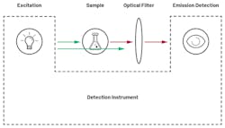
In a fluorescence-based IVD test, a sample containing fluorescent labels is excited with the light of a specific wavelength as shown by the green arrow in Figure 1. If the sample contains the analyte of interest, the fluorescent labels react to the excitation by emitting a light of a lower energy level.
For example, in Figure 1, the fluorescent labels in the sample react by emitting red light. This emitted light is the fluorescence signal that needs to be detected to determine the presence, and possibly the amount, of analyte in the sample.
A fluorescence-based diagnostic test will have a threshold of what’s considered reportable fluorescence. A fluorescence signal below the threshold level cannot confidently indicate the presence of the analyte in the sample. The electronics in the diagnostic detection instrument, along with other factors, contribute to the background noise, which forces the threshold higher.
To reduce the threshold level and consequently achieve better sensitivity without sacrificing selectivity, a careful design of the optical detection system is needed to ensure that the electronic receive chain doesn’t contribute to the background noise level.
PoC Fluorescence-Detection System
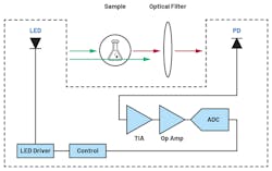
A typical PoC diagnostic fluorescence-detection system employs a light-emitting diode (LED) to generate the excitation light and a photodiode (PD) to detect the fluorescence emission from the sample. The PD generates an electrical current that’s proportional to the intensity of the fluorescence signal, which can be extremely weak. The PD current is often very small relative to the noise floor, necessitating careful electronic design to achieve high-sensitivity detection without sacrificing selectivity.
Figure 2 shows the main elements of a typical PoC fluorescence-detection system. The current signal from the PD is converted to a voltage signal by the transimpedance amplifier (TIA). The voltage signal is digitized by the analog-to-digital converter (ADC) and translated into a corresponding level of fluorescence.
Performance Needs of a Fluorescence-Detection PoC System
Designers of PoC systems strive to achieve maximum diagnostic sensitivity without sacrificing selectivity. Regarding PoC instruments, this goal translates into the requirement of reliably discerning, very low PD current in response to LED excitation.
For example, a high-sensitivity system must be able to detect PD currents on the order of picoamperes in response to LED excitation currents on the order of 100 mA. That is, the system must be able to detect PD fluorescence given approximately 140 dB of optical attenuation.
To achieve such performance, a combination of electronic and system design considerations is necessary. The design of the analog front end (AFE) for the PD is particularly important. Because the PD current is often very weak relative to the noise floor, the TIA must have a high gain and low input bias current. Additional important parameters are low TIA input offset voltage as well as a minimum distance between the PD and TIA.
The system design is also very important to achieve high-sensitivity detection. Fluorescence detection must be synchronized with the LED excitation, hence the need for a controller that ensures this synchronicity.
Averaging of multiple fluorescence readings is often required to discern the weak PD current signal from the noise floor. This averaging technique is an important function of the system controller. Ambient light and drift in LED lighting can contribute to a system error. A controller that allows for the rejection of ambient light and accounts for the impact of drift in LED lighting can enable an overall system performance advantage.
The Benefits of an Integrated Optical Front-End Receiver
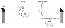
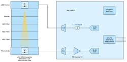
When designing the electronic receiver chain for a PoC reader, two distinct architecture choices are available: a fully discrete solution (Fig. 2) or the use of an integrated optical front end (Fig. 3).
The first clear benefit of an integrated solution is simplified system design. The challenge of synchronizing the fluorescence detection with the LED excitation is removed—it’s handled internally by the optical front end. Integrated optical front ends also provide a more compact solution with fewer electronic components, thus reducing BOM and supply management complexity while enabling a smaller end device.
However, the most critical benefit of an integrated optical front end is the ability to adjust key configuration parameters, such as photodiode, LED driver, and signal filtering configuration, via firmware. Programmability isn’t available with a discrete solution without new hardware being developed.
This type of configurability is critical when trying to adapt a platform over time to operate with new or modified assays. As new variants and diseases are frequently added to testing menus, creating a receiver platform that can be modified to accommodate new assays, without the need for hardware modifications, is highly advantageous.
Integrated optical front ends offer clear advantages, though—determining the performance of an optical front end in low-light fluorescent applications isn’t a trivial task.
Comparing signal-to-noise ratio (SNR) figures between integrated optical front ends doesn’t give a true sense of the real-life performance of an optical receiver. As the levels of light are typically low, the absolute noise floor of the optical front ends is the critical parameter, rather than the SNR.
With the timescale associated with fluorescent measurements, averaging can be employed to reduce this noise floor, though the 1/f noise component places a practical limit on what improvements can be achieved through averaging. Therefore, absolute dark current noise, particularly flicker noise, is the dominant factor. The dark current noise of a full system, including the PD, isn’t characterized in the datasheet of many integrated optical AFEs and must be measured separately.
ADI’s Integrated Front Ends
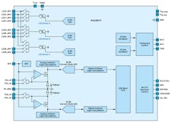
Integrated optical front ends developed by Analog Devices, such as the MAX86171, are suited for PoC fluorescence applications. The integration of the analog signal chain alongside the digital controller makes possible a single-IC solution for implementing an optical receiver. The MAX86171 contains signal-conditioned photodiode inputs, a 19-bit charge integrating ADC, low-noise LED drivers, and a FIFO-buffered serial interface (Fig. 4).
With nine LED channels and four PD channels, the AFE supports multiassay testing and adequate channels for future testing expansion without hardware upgrades. Programming over SPI or I2C allows for the fine-tuning of parameters to a given assay, such as integration time, averaging, and dynamic range. A FIFO enables MCUs to remain in sleep mode while taking measurements, extending battery life in handheld PoC systems.
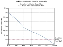
In addition, the high-performance and low-noise nature of the device can lead to development of a high-sensitivity detection system. Averaging and low 1/f noise enable a dark current noise of just 11 pA rms for the whole optical signal chain with a photodiode area of 7.5 mm2. As a result, low photodiode currents can be reliably detected in the range of 1 to 10 pA, typical for low-yield fluorescence applications. Furthermore, its PSRR and ambient light rejection features ease the system engineer’s burden while designing the power-supply unit and mechanical enclosure.
To validate the performance of the MAX86171, an LED driven by the front end was passed through varying levels of neutral-density (ND) optical filters and received via a photodiode by the device (Fig. 5). By increasing the density of the ND filters, the optical attenuation can be varied from 40 dB (ND2) to 140 dB (ND7), simulating reducing fluorescent yields in a PCR or LAMP-based detection system.
Such performance exceeds what’s typically required in PoC instruments and allows the full potential of the biosensor or chemistry to be reached. The internal registers of the MAX86171 make it possible to program parameters such as pulse width, pulse intensity, photodiode gain, and photodiode biasing via firmware. Signal filtering, averaging, and ambient-light rejection options are also available to optimize optical detection. Together, this helps maximize flexibility to adapt to new assays without the need for hardware rework.
Conclusion
Designing a circuit for an IVD system requires careful attention to both the electronic section and system design to ensure that high-sensitivity detection is achieved without sacrificing selectivity. Identifying the weak electronic signal is critical when creating a system that can showcase the full potential of the biosensor or chemistry, and ultimately results in a device with accurate diagnostic results.

